A gated bipolar-field effect compound element semiconductor-based vdmos

A semiconductor and field-effect technology, applied in the field of vertical double-diffused metal-oxide-semiconductor transistors

Active Publication Date: 2021-04-13
XIDIAN UNIV
View PDF6 Cites 0 Cited by
  • Summary
  • Abstract
  • Description
  • Claims
  • Application Information

AI Technical Summary

Problems solved by technology

However, in the on state, due to the short circuit between the base region and the source region, the parasitic bipolar transistor is still not turned on, and the device can only conduct electricity in the normally turned on channel

Method used


Image

  • A gated bipolar-field effect compound element semiconductor-based vdmos
  • A gated bipolar-field effect compound element semiconductor-based vdmos

Examples


Embodiment Construction

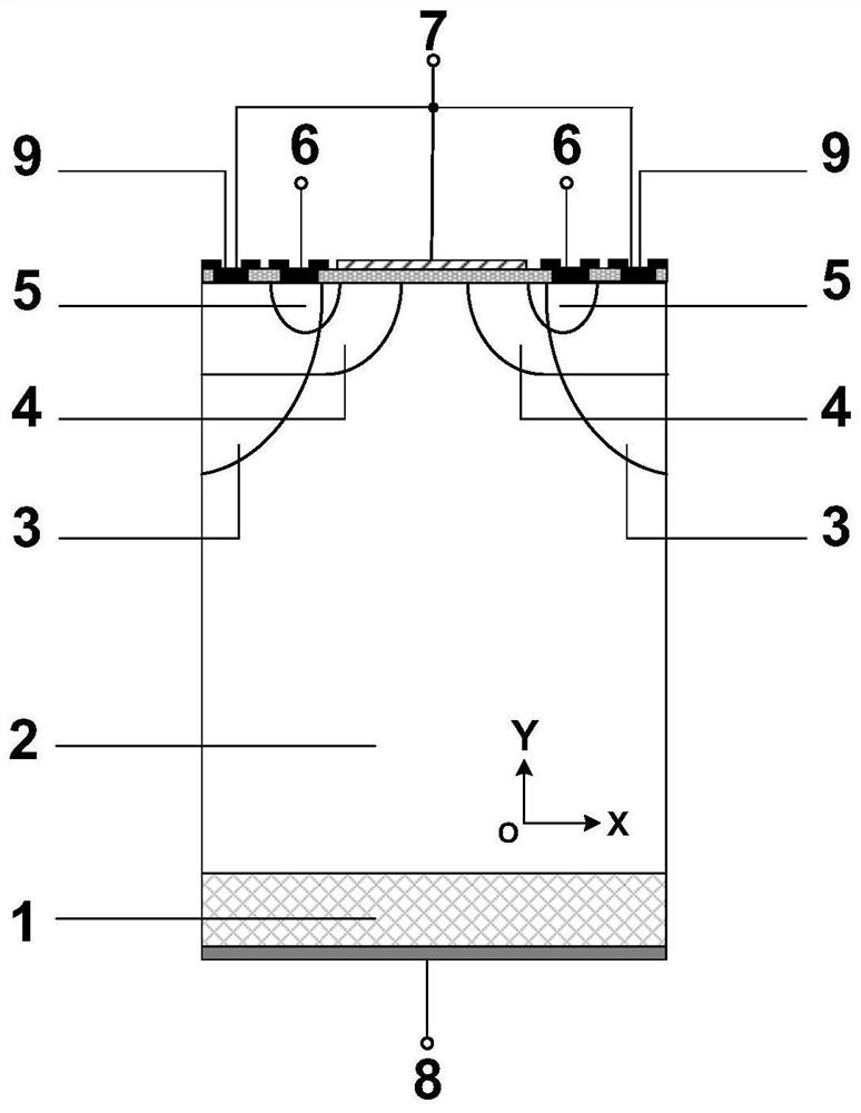
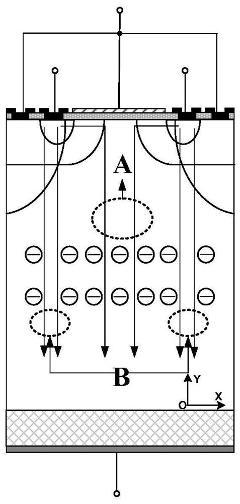
[0026] Such as figure 1 As shown, the gate-controlled bipolar-field-effect compound element semiconductor-based vertical double-diffused metal-oxide-semiconductor transistor includes:

[0027] Elemental semiconductor substrate 1, the doping concentration is the concentration of general elemental semiconductor single crystal material, the typical value is 1×10 13 cm -3 ~1×10 15 cm -3 ;

[0028] The drift region 2 is epitaxially formed on the substrate, and the doping concentration of the drift region is 3×10 15 cm -3 ;

[0029] a gate insulating layer formed on the surface of the drift region, and forming a gate 7 above the gate insulating layer;

[0030] A heavily doped region 3 and a base region 4 are formed on the drift region; wherein, the doping concentration of the base region is 5×10 16 cm -3 , the doping concentration in the heavily doped region is 1×10 16 cm -3 ;

[0031] forming a source region 5 on the base region and simultaneously forming a channel on s...


PUM


Abstract

The invention discloses a gate-controlled bipolar-field effect composite element semiconductor-based VDMOS. The substrate and epitaxy-generated drift region of this structure are both elemental semiconductor materials, the base is isolated from the source, and electrically connected to the gate, and the connection material between the base and the gate is a semiconductor material, so that the base access voltage When the base potential is greater than the gate potential, the gate potential is greater than the base potential when the gate is connected to the voltage, and it is satisfied that: when the gate is connected to the voltage, the voltage obtained by the base region makes the parasitic bipolar transistor of the device turn on. Compared with the traditional device, the invention greatly increases the conduction current of the device and reduces the conduction resistance of the device while ensuring the same breakdown voltage of the device.

Description

technical field [0001] The invention relates to the technical field of semiconductor power devices, in particular to a vertical double diffused metal oxide semiconductor transistor (VDMOS). Background technique [0002] Power Metal Oxide Semiconductor Field Effect Transistor (MOSFET) is a new generation of semiconductor power switching device developed on the basis of MOS integrated circuit technology. It has made great progress in the past 20 years. It started with LDMOS structure and experienced VVMOS, VUMOS, VDMOS. The evolution of structures such as , EXTFET, etc. is still dominated by VDMOS structures. Vertical double diffused metal oxide semiconductor (VDMOS) devices have a series of unique features such as high input impedance, fast switching speed, high operating frequency, voltage control, and good thermal stability. It has been widely used in switching steady-state power supplies, high-frequency heating, computer interface circuits, and power amplifiers. [0003] ...

Claims


Application Information

Patent Timeline
Patent Type & Authority Patents(China)
IPC IPC(8): H01L29/78H01L29/167H01L29/10
CPCH01L29/1095H01L29/167H01L29/7802
Inventor 段宝兴董自明杨银堂
Owner XIDIAN UNIV
Why Eureka
Try Eureka