


Quick Research
Generate reliable direction feasibility study reports for your R&D in just a few steps.

Technical Q&A
Discover and master advanced knowledge NOW. Basics, ideas, possibilities, all at once.

Find Solutions
As an expert in R&D theories, this can generate solutions to your technical problems instantly.

Evaluate Feasibility
Analyze your overall solution with one click, know your potential R&D risks in advance.

Monitor Landscape
Get weekly tech updates, stay abreast of the latest tech innovations and key insights.
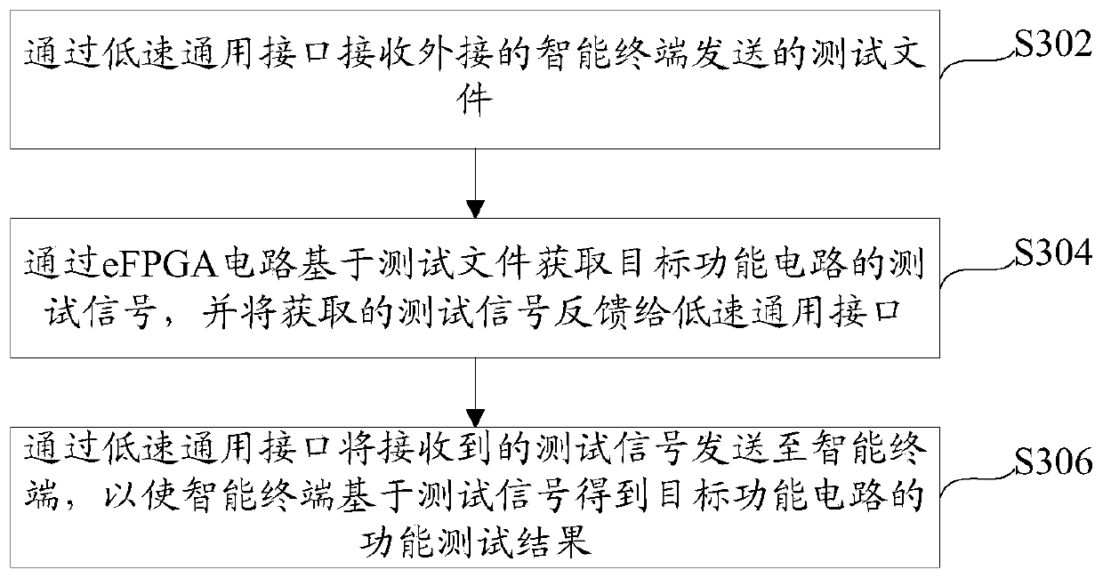
Integrated chip and test method thereof
An integrated chip and chip technology, applied in the direction of digital circuit testing, electronic circuit testing, electrical measurement, etc., can solve the problem that the high-speed signal of the chip cannot pass the function test, signal rate limitation, etc.
- Summary
- Abstract
- Description
- Claims
- Application Information
AI Technical Summary
Problems solved by technology
Method used
Image


Examples
Embodiment Construction
[0023] In order to make the purpose, technical solutions and advantages of the embodiments of the present invention clearer, the technical solutions of the present invention will be clearly and completely described below in conjunction with the embodiments. Obviously, the described embodiments are part of the embodiments of the present invention, not all of them. the embodiment. Based on the embodiments of the present invention, all other embodiments obtained by persons of ordinary skill in the art without making creative efforts belong to the protection scope of the present invention.
[0024] At present, when testing an integrated chip (ASIC, Application Specific Integrated Circuit), usually the digital IO interface is not specially designed for the test circuit of the chip, and is multiplexed with the functional IO interface of the chip itself, but through IO multiplexing There are relatively large restrictions when testing the function of the chip. First, due to the limite...
PUM
 Abstract
Description
Claims
Application Information
 - R&D Engineer
- R&D Manager
- IP Professional
- Industry Leading Data Capabilities
- Powerful AI technology
- Patent DNA Extraction
Browse by: Latest US Patents, China's latest patents, Technical Efficacy Thesaurus, Application Domain, Technology Topic, Popular Technical Reports.
© 2024 PatSnap. All rights reserved.Legal|Privacy policy|Modern Slavery Act Transparency Statement|Sitemap|About US| Contact US: help@patsnap.com