Image sensor and forming method thereof

An image sensor and graphics technology, applied in the direction of electric solid devices, semiconductor devices, electrical components, etc., can solve the problems of easy saturation of white pixels and lower utilization rate of pixel area, etc. Effect

Inactive Publication Date: 2019-08-23
HUAIAN IMAGING DEVICE MFGR CORP
View PDF4 Cites 1 Cited by
  • Summary
  • Abstract
  • Description
  • Claims
  • Application Information

AI Technical Summary

Problems solved by technology

[0005] The technical problem to be solved by the technical solution of the present invention is: in view of the fact that the white pixels in the existing image sensor are easily saturated, the utilization rate of the pixel area is reduced by shielding part of the incoming light to prevent the white pixels from being saturated in advance

Method used


Image

  • Image sensor and forming method thereof
  • Image sensor and forming method thereof
  • Image sensor and forming method thereof

Examples


no. 1 example

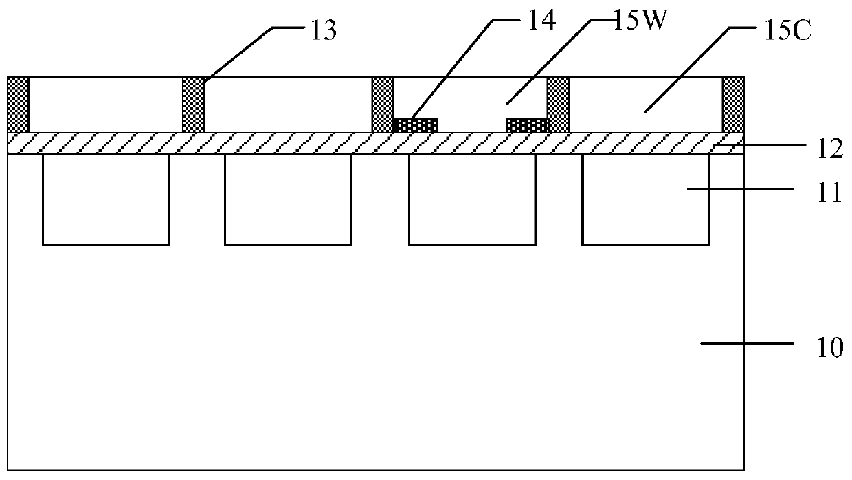
[0033] Figure 2 to Figure 6 is a schematic cross-sectional structure diagram corresponding to each step in the method for forming an image sensor according to the first embodiment of the present invention.

[0034] refer to figure 2 First, a semiconductor substrate 100 formed with discretely arranged photodiodes 110 is provided, the semiconductor substrate 100 includes several pixel regions, the several pixel regions have white pixel regions, and the photodiodes 110 correspond to each pixel region.

[0035] In this embodiment, the semiconductor substrate 100 may be a silicon substrate, or germanium, silicon germanium, silicon carbide, gallium arsenide, or indium gallium, or a silicon-on-insulator substrate or a germanium-on-insulator substrate. The substrate, or the substrate on which the epitaxial layer is grown. The semiconductor substrate 100 includes a photodiode 110 for converting received optical signals into electrical signals.

[0036] In this embodiment, accordin...

no. 2 example

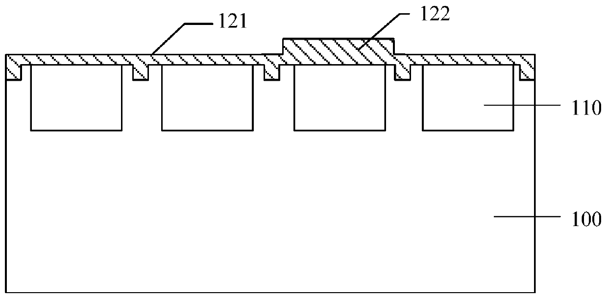
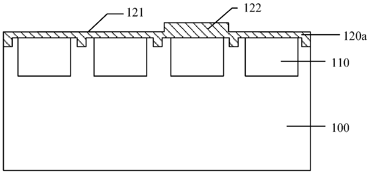
[0067] Figure 7 to Figure 11 is a schematic cross-sectional structure diagram corresponding to each step in the method for forming an image sensor according to the second embodiment of the present invention.

[0068] refer to Figure 7 Firstly, a semiconductor substrate 200 formed with discretely arranged photodiodes 210 is provided, the semiconductor substrate 200 includes several pixel regions, the several pixel regions include white pixel regions, and the photodiodes 210 correspond to each pixel region.

[0069] In this embodiment, the semiconductor substrate 200 may be a silicon substrate, or germanium, silicon germanium, silicon carbide, gallium arsenide, or indium gallium, or a silicon-on-insulator substrate or a germanium-on-insulator substrate. The substrate, or the substrate on which the epitaxial layer is grown. The semiconductor substrate 200 includes a photodiode 210 for converting received optical signals into electrical signals.

[0070] In this embodiment, acc...


PUM


Abstract

The technical scheme of the invention discloses an image sensor and a forming method thereof, and the method comprises the steps: providing a semiconductor substrate which comprises a plurality of pixel regions, wherein the plurality of pixel regions comprise white pixel regions; forming a first insulation structure and a second insulation structure on the semiconductor substrate, wherein the first insulation structure is located in a non-white pixel region, and the second insulation structure is located in the white pixel region; etching the surface of the second insulation structure to forma concave surface; forming first light shielding layers which are arranged separately on the first insulation structure; forming a second light shielding layer, wherein the second light shielding layer covers the surface of the second insulation structure outside the concave surface; forming a color filter layer corresponding to each pixel area on the first insulation structure between the first light shielding layers; and forming a white color filter layer on the concave surface between the second light shielding layers or on the second light shielding layers and the concave surface. The image quality of the image sensor is improved.

Description

technical field [0001] The invention relates to the technical field of semiconductor manufacturing, in particular to a CMOS image sensor and a forming method thereof. Background technique [0002] An image sensor is a device that converts an optical image into an electrical signal. With the development of the computer and communication industries, the demand for high-performance image sensors is increasing. These high-performance image sensors are widely used in digital cameras, video recorders, personal communication systems (PCS), game consoles, security cameras, and medical miniature cameras. various fields. [0003] Image sensors are generally of two types, Charge Coupled Device (CCD) sensors and CMOS Image Sensors (CMOS Image Sensors, CIS). Compared with CCD image sensors, CMOS image sensors have the advantages of high integration, low power consumption, and low production cost. In the traditional CMOS photosensitive element, the photosensitive diode is located behin...

Claims


Application Information

Patent Timeline
Patent Type & Authority Applications(China)
IPC IPC(8): H01L27/146
CPCH01L27/14621H01L27/14623H01L27/14627H01L27/1463H01L27/14645H01L27/14683H01L27/14687
Inventor 陈腾飞孟宪宇吴宗祐林宗贤
Owner HUAIAN IMAGING DEVICE MFGR CORP
Why Eureka
Try Eureka