Temperature sensor, electrode and temperature sensitive film connecting structure and preparation method
A connection structure and electrode structure technology, which is applied to the connection structure of the electrode and the temperature-sensitive film in the resistive deep-low temperature sensor and its preparation field, can solve the problems of large measured value, decreased sensor sensitivity, increased oxidation, etc., to improve the effective The effect of resistance output, improving the accuracy of test temperature and reducing test error
- Summary
- Abstract
- Description
- Claims
- Application Information
AI Technical Summary
Problems solved by technology
Method used
Image

Examples
Embodiment 1
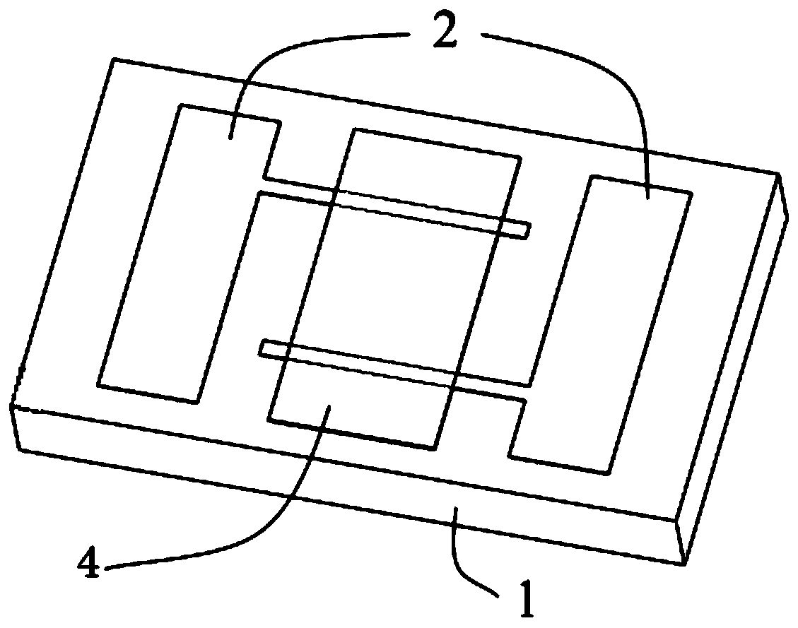
[0028] Such as figure 1 As shown in the figure, the figure is a structural schematic diagram of the connection structure between the electrode and the temperature-sensitive film in a resistive deep-low temperature sensor. The figure includes an insulating substrate 1, an electrode 2, and a temperature-sensitive film layer 4, and the electrodes are sequentially arranged on the insulating substrate 1. 2. The temperature sensitive film layer 4 , the electrode transition layer 3 is arranged between the electrode 2 and the temperature sensitive film layer 4 .
[0029] The present invention is different from the traditional process of preparing electrodes on the sensitive film. Firstly, the electrodes are prepared on the insulating substrate, and the temperature sensitive film is prepared on the electrodes. The effective resistance output of the sensitive film reduces the test error and improves the test temperature accuracy of the deep low temperature temperature sensor.
[0030] ...
Embodiment 2
[0042] The material of the insulating base 1 is silicon oxide substrate, the material of the electrode 2 is copper, and the material of the temperature-sensitive film layer 4 is zirconium oxynitride. An electrode transition layer 3 is arranged between the film layers 4 . The material of the electrode transition layer 3 is chromium.
[0043] A flow chart of a method for manufacturing a connection structure between an electrode and a temperature-sensitive film in a resistive deep-low temperature sensor, specifically comprising the following steps:
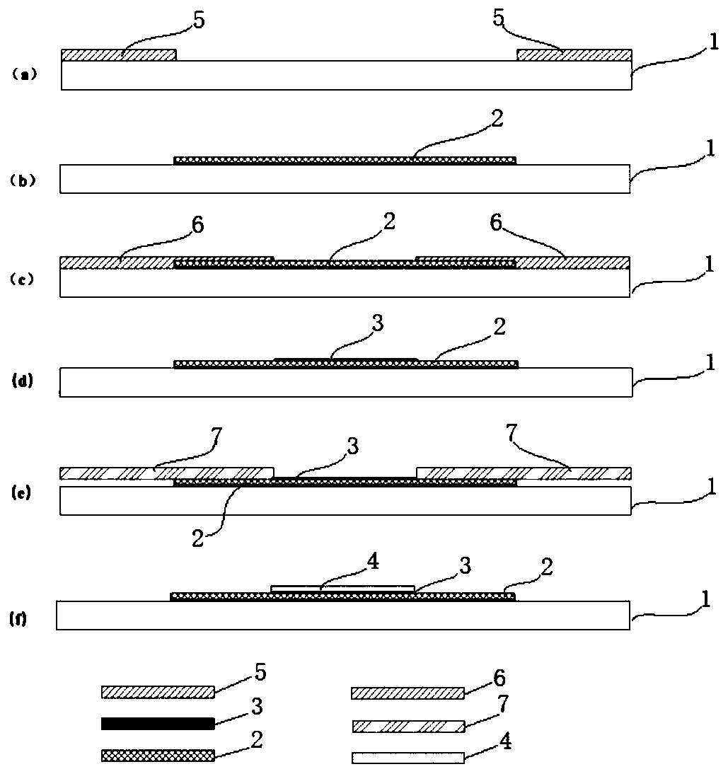
[0044] (1) Fabricate a patterned electrode on the insulating substrate 1, and its micro-machining process is gelling, photolithography, development, sputtering and lift-off process. Specifically refers to: in the present embodiment, the material of the insulating base 1 is a silicon oxide substrate, such as figure 2 As shown in (a), 5 μm of photoresist I5 is thrown on the insulating substrate 1, and the photoresist I5 is patterned...
Embodiment 3
[0049] The material of the insulating substrate 1 is alumina ceramics, the material of the electrode 2 is gold, and the material of the temperature sensitive film layer 4 is niobium oxynitride. The electrode 2 and the temperature sensitive film layer 4 are arranged in sequence on the insulating substrate 1. An electrode transition layer 3 is arranged between the layers 4 . The material of the electrode transition layer 3 is titanium.
[0050] A flow chart of a method for manufacturing a connection structure between an electrode and a temperature-sensitive film in a resistive deep-low temperature sensor, specifically comprising the following steps:
[0051] (1) Fabricate a patterned electrode on the insulating substrate 1, and its micro-machining process is gelling, photolithography, development, sputtering and lift-off process. Specifically refers to: in the present embodiment, the material of the insulating base 1 is alumina ceramics, such as figure 2 As shown in (a), 5 μm...
PUM
| Property | Measurement | Unit |
|---|---|---|
| thickness | aaaaa | aaaaa |
| thickness | aaaaa | aaaaa |
| thickness | aaaaa | aaaaa |
Abstract
Description
Claims
Application Information
 - Generate Ideas
- Intellectual Property
- Life Sciences
- Materials
- Tech Scout
- Unparalleled Data Quality
- Higher Quality Content
- 60% Fewer Hallucinations
Browse by: Latest US Patents, China's latest patents, Technical Efficacy Thesaurus, Application Domain, Technology Topic, Popular Technical Reports.
© 2025 PatSnap. All rights reserved.Legal|Privacy policy|Modern Slavery Act Transparency Statement|Sitemap|About US| Contact US: help@patsnap.com