


Quick Research
Generate reliable direction feasibility study reports for your R&D in just a few steps.

Technical Q&A
Discover and master advanced knowledge NOW. Basics, ideas, possibilities, all at once.

Find Solutions
As an expert in R&D theories, this can generate solutions to your technical problems instantly.

Evaluate Feasibility
Analyze your overall solution with one click, know your potential R&D risks in advance.

Monitor Landscape
Get weekly tech updates, stay abreast of the latest tech innovations and key insights.
Transmitting signal interference optimization method, display module and terminal
A technology for transmitting signals and optimizing methods, which is applied in the field of communication and can solve problems such as antenna interference
- Summary
- Abstract
- Description
- Claims
- Application Information
AI Technical Summary
Problems solved by technology
Method used
Image

Examples
no. 1 example
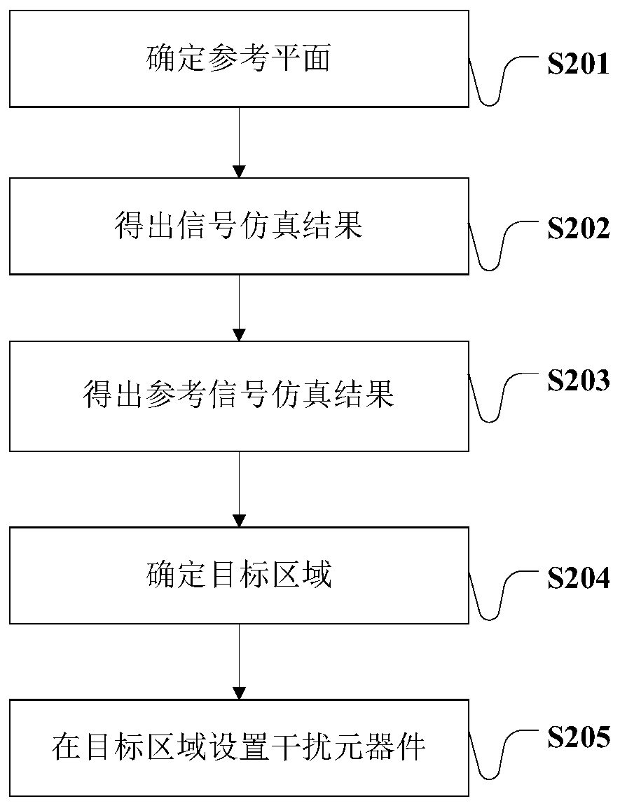
[0062] figure 2 The basic flowchart of a transmission signal interference optimization method provided in this embodiment, the transmission signal interference optimization method includes:
[0063] S201. Determine a reference plane.
[0064] In this step, the reference plane is the plane on which the circuit board is set, and the circuit board may be a PCB circuit board, a flexible PCB circuit board, a thin film circuit, and the like.
[0065] S202. Obtain a signal simulation result.
[0066] In this step, a transmission signal of a specific frequency is loaded on the antenna, and a signal simulation is performed on the transmission signal to obtain a signal simulation result of the transmission signal.
[0067] S203. Obtain a reference signal simulation result.
[0068] After the reference plane is determined, the simulation result of the reference signal located on the reference plane is intercepted from the simulation result of the signal.
[0069] S204. Determine the...
no. 2 example
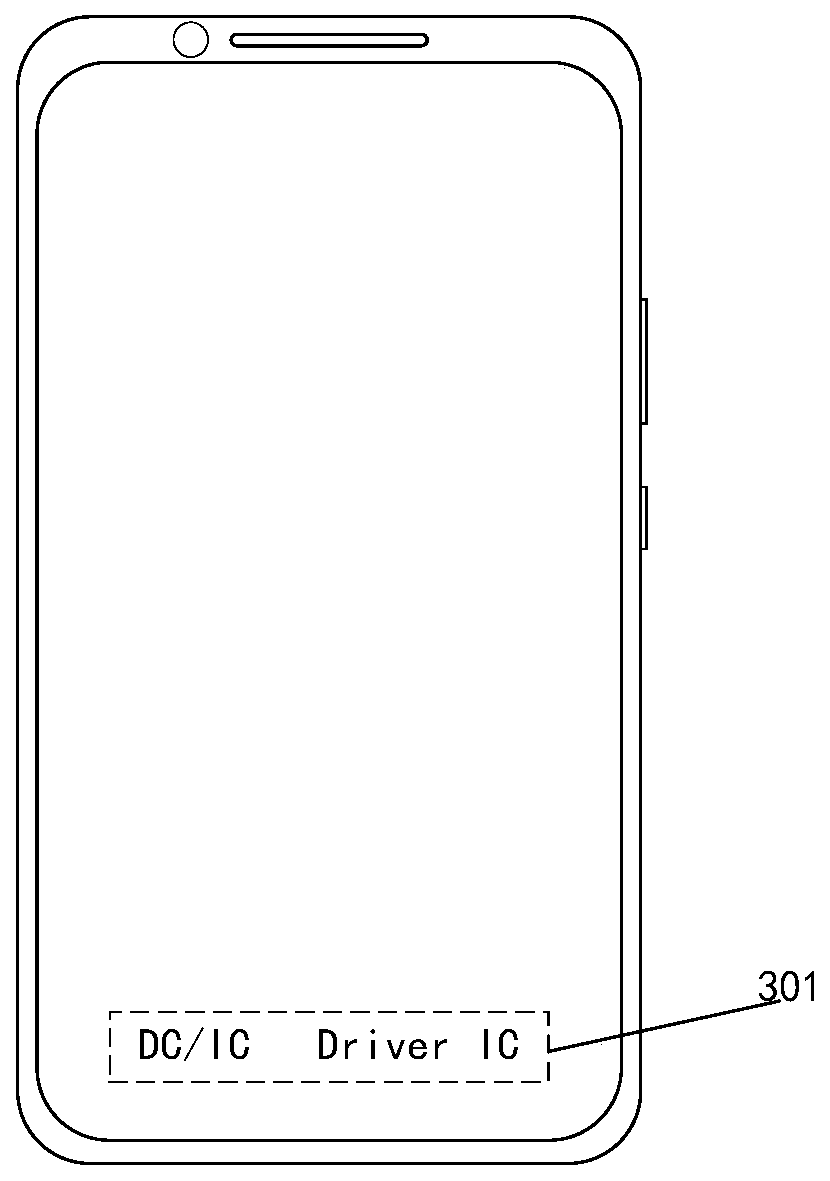
[0088] This embodiment shows an example of the application of the present invention on smart phones. In current smart phones, with the emergence of full screens, the area occupied by the display area of the front display screen of the mobile phone is getting higher and higher. The distance between the screen driver IC on the cable at the lower end of the display and the antenna at the bottom of the mobile phone is getting closer and closer. The function of the current liquid crystal element is similar to that of a capacitor. The display of the image requires a switching voltage to continuously operate the element, so the driver IC has a built-in DC / DCpumping circuit converter to generate the high and low level VGH, VGL, and common frequency of the element switch. Generally, it is 600K or 800KHz. Since the LCD driver IC contains an oscillator to generate various clock working signals when the screen is bright, the driver IC contains many nonlinear devices. When the antenna of...
no. 3 example
[0114] This embodiment also provides a display module, and the display module includes: a driver IC, an FPC cable carrying the driver IC, and a backlight module;
[0115] The FPC cable is set on the back of the backlight module, and the driver IC is set on the target area on the FPC cable;
[0116] The target area is determined by the transmission signal interference optimization method in the first embodiment to the second embodiment in the embodiments of the present invention.
[0117] This embodiment also provides a terminal, which includes an antenna and the above-mentioned display screen module;
[0118] The antenna is an omnidirectional antenna, which is arranged under the display module and close to the position of the display module.
PUM
 Abstract
Description
Claims
Application Information
 - R&D Engineer
- R&D Manager
- IP Professional
- Industry Leading Data Capabilities
- Powerful AI technology
- Patent DNA Extraction
Browse by: Latest US Patents, China's latest patents, Technical Efficacy Thesaurus, Application Domain, Technology Topic, Popular Technical Reports.
© 2024 PatSnap. All rights reserved.Legal|Privacy policy|Modern Slavery Act Transparency Statement|Sitemap|About US| Contact US: help@patsnap.com