Quantum plasmon material as well as preparation method and application thereof
A plasmon and quantum technology, applied in the field of optical coupling, can solve problems such as complex methods, and achieve the effects of simple preparation methods and complex preparation methods.
- Summary
- Abstract
- Description
- Claims
- Application Information
AI Technical Summary
Problems solved by technology
Method used
Image
Examples
preparation example Construction
[0023] The invention provides a method for preparing a quantum plasmonic material, comprising the following steps:
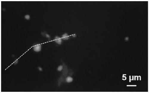
[0024] (1) Ultrasonic treatment after mixing the silver nanowire aqueous solution and the CdSe-ZnS quantum dot aqueous solution to obtain a mixed solution;
[0025] (2) Spin-coat the mixed solution obtained in the step (1) on the substrate under vacuum conditions to obtain a quantum plasmonic material.
[0026] In the invention, the silver nanowire aqueous solution and the CdSe-ZnS quantum dot aqueous solution are mixed and then ultrasonically treated to obtain a mixed solution.
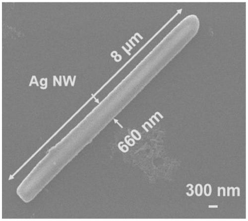
[0027] In the present invention, the diameter of the silver nanowires is preferably 120-860nm, more preferably 150-800nm, more preferably 300-700nm; the concentration of the raw silver nanowire aqueous solution is preferably 1-10mg / mL, further Preferably it is 2-8 mg / mL, more preferably 4-6 mg / mL. In the present invention, the mass concentration of silver nanowires in the mixed solut...
Embodiment 1
[0040] (1) configuring the silver nanowires into an aqueous solution of silver nanowires with a concentration of 1 mg / mL;
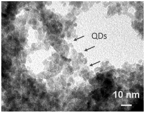
[0041] (2) CdSe-ZnS quantum dots with a diameter of 5 nm are configured into an aqueous solution of quantum dots with a concentration of 1 μmol / L;
[0042] (3) Mix 100 μL of the above-mentioned silver nanowire aqueous solution with 50 μL of the above-mentioned quantum dot aqueous solution, and then add 1 mL of distilled water to dilute to obtain a mixed solution; ultrasonically treat the mixed solution for 10 minutes, so that a mixed solution suitable for forming a uniform coating layer can be obtained;
[0043](4) Use a pipette to take out 100 μL of the mixed solution, drop it on the cleaned and dried silicon wafer, place the silicon wafer on the stage of the spin coater, draw a vacuum, and cover the glass of the spin coater. Cover, adjust the spin coating speed, perform low speed spin coating and high speed spin coating in sequence, the speed of low spe...
Embodiment 2
[0045] (1) configuring the silver nanowires into a silver nanowire aqueous solution with a concentration of 5 mg / mL;
[0046] (2) CdSe-ZnS quantum dots with a diameter of 6 nm are configured into a quantum dot aqueous solution with a concentration of 2 μmol / L;
[0047] (3) Mix the above-mentioned silver nanowire aqueous solution and the above-mentioned quantum dot aqueous solution to obtain a mixed solution, the mass concentration of the silver nanowire in the mixed solution is 8wt%, and the mass concentration of the quantum dots in the mixed solution is 4wt%; the mixed solution is ultrasonically treated for 12min , can obtain the mixed solution that is suitable for forming uniform coating layer like this;
[0048] (4) Use a pipette to take out 100 μL of the mixed solution, drop it on the cleaned and dried silicon wafer, place the silicon wafer on the stage of the spin coater, draw a vacuum, and cover the glass of the spin coater. Cover, adjust the spin-coating speed, and per...
PUM
| Property | Measurement | Unit |
|---|---|---|
| diameter | aaaaa | aaaaa |
| diameter | aaaaa | aaaaa |
| thickness | aaaaa | aaaaa |
Abstract
Description
Claims
Application Information
 - R&D Engineer
- R&D Manager
- IP Professional
- Industry Leading Data Capabilities
- Powerful AI technology
- Patent DNA Extraction
Browse by: Latest US Patents, China's latest patents, Technical Efficacy Thesaurus, Application Domain, Technology Topic, Popular Technical Reports.
© 2024 PatSnap. All rights reserved.Legal|Privacy policy|Modern Slavery Act Transparency Statement|Sitemap|About US| Contact US: help@patsnap.com


