Fabrication method of transparent conductive film structure

A technology of transparent conductive film and production method, which is applied in the direction of equipment for manufacturing conductive/semiconductive layer, cable/conductor manufacturing, circuit, etc., can solve the problem of high production cost, achieve fast grinding rate, reduce production cost, and ensure The effect of the zero-valent valence state

Active Publication Date: 2020-05-12
SUZHOU LANPEI OPTOELECTRONICS TECH CO LTD
View PDF8 Cites 0 Cited by
  • Summary
  • Abstract
  • Description
  • Claims
  • Application Information

AI Technical Summary

Problems solved by technology

[0004] In view of the shortcomings of the above-mentioned prior art, the purpose of the present invention is to provide a method for manufacturing a transparent conductive film structure, which is used to solve the problem of high production cost when using silver paste to prepare a transparent conductive film structure in the prior art. question

Method used


Image

  • Fabrication method of transparent conductive film structure
  • Fabrication method of transparent conductive film structure
  • Fabrication method of transparent conductive film structure

Examples


Embodiment Construction

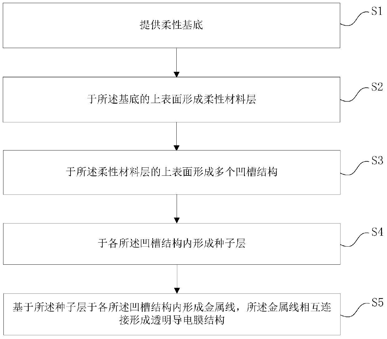
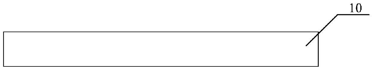
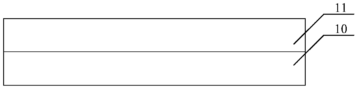
[0056] The following specific examples illustrate the implementation of the present invention. Those skilled in the art can easily understand other advantages and effects of the present invention from the content disclosed in this specification.

[0057] See Figure 1 to Figure 7 . It should be noted that the structure, ratio, size, etc. shown in the accompanying drawings in this specification are only used to match the content disclosed in the specification for the understanding and reading of those familiar with this technology, and are not intended to limit the implementation of the present invention Limited conditions, so it has no technical significance. Any structural modification, proportional relationship change or size adjustment should still fall under the present invention without affecting the effects and objectives that can be achieved by the present invention. The disclosed technical content must be within the scope of coverage. At the same time, the terms such as ...


PUM

PropertyMeasurementUnit
particle diameteraaaaaaaaaa
depthaaaaaaaaaa

Abstract

The invention provides a fabrication method of a transparent conductive film structure. The fabrication method comprises the following steps of providing a flexible substrate; forming a flexible material layer on an upper surface of the flexible substrate; forming a plurality of groove structures on an upper surface of the flexible material layer; forming seed layers in the groove structures; andforming a metal line in each groove structure according to the seed layer, wherein the metal lines are connected to form the transparent conductive film structure. By the seed layer, relatively high reduction performance of iron powder can be enabled to be maintained, so that metal line breakage formed by the seed layers is prevented, and the performance of the formed transparent conductive film structure is further ensured.

Description

Technical field [0001] The invention belongs to the technical field of touch control, and particularly relates to a method for manufacturing a transparent conductive film structure. Background technique [0002] The transparent conductive film structure such as metal grid contained in the touch screen (also known as the touch screen) is formed by forming a corresponding groove structure on the surface of the flexible material layer, and then filling the groove structure with silver through a process such as scratch printing. Paste such as paste forms a conductive layer, thereby obtaining a transparent conductive film structure. [0003] However, silver paste is a precious metal paste, and the use of silver paste to form the seed layer will inevitably lead to excessive production costs. Summary of the invention [0004] In view of the above-mentioned shortcomings of the prior art, the purpose of the present invention is to provide a method for manufacturing a transparent conductive ...

Claims


Application Information

Patent Timeline
Patent Type & Authority Patents(China)
IPC IPC(8): G06F3/041H01B13/00
CPCH01B13/0026
Inventor 谢自民冯波郭向阳陈春明平财明林涛
Owner SUZHOU LANPEI OPTOELECTRONICS TECH CO LTD
Why Eureka
Try Eureka