
Transfer circuit, shift register, gate driver, display panel, and flexible substrate

A transmission circuit and input circuit technology, applied in transmission circuits, shift registers, gate drivers, display panels, and flexible substrates, can solve problems such as potential rise and accumulation

Inactive Publication Date: 2019-07-16
JOLED INC
View PDF5 Cites 0 Cited by
  • Summary
  • Abstract
  • Description
  • Claims
  • Application Information

AI Technical Summary

Problems solved by technology

Therefore, in a shift register in which a plurality of these register circuits are connected, potential rises and accumulations during repeated transmission of control signals may cause malfunctions.

Method used


Image

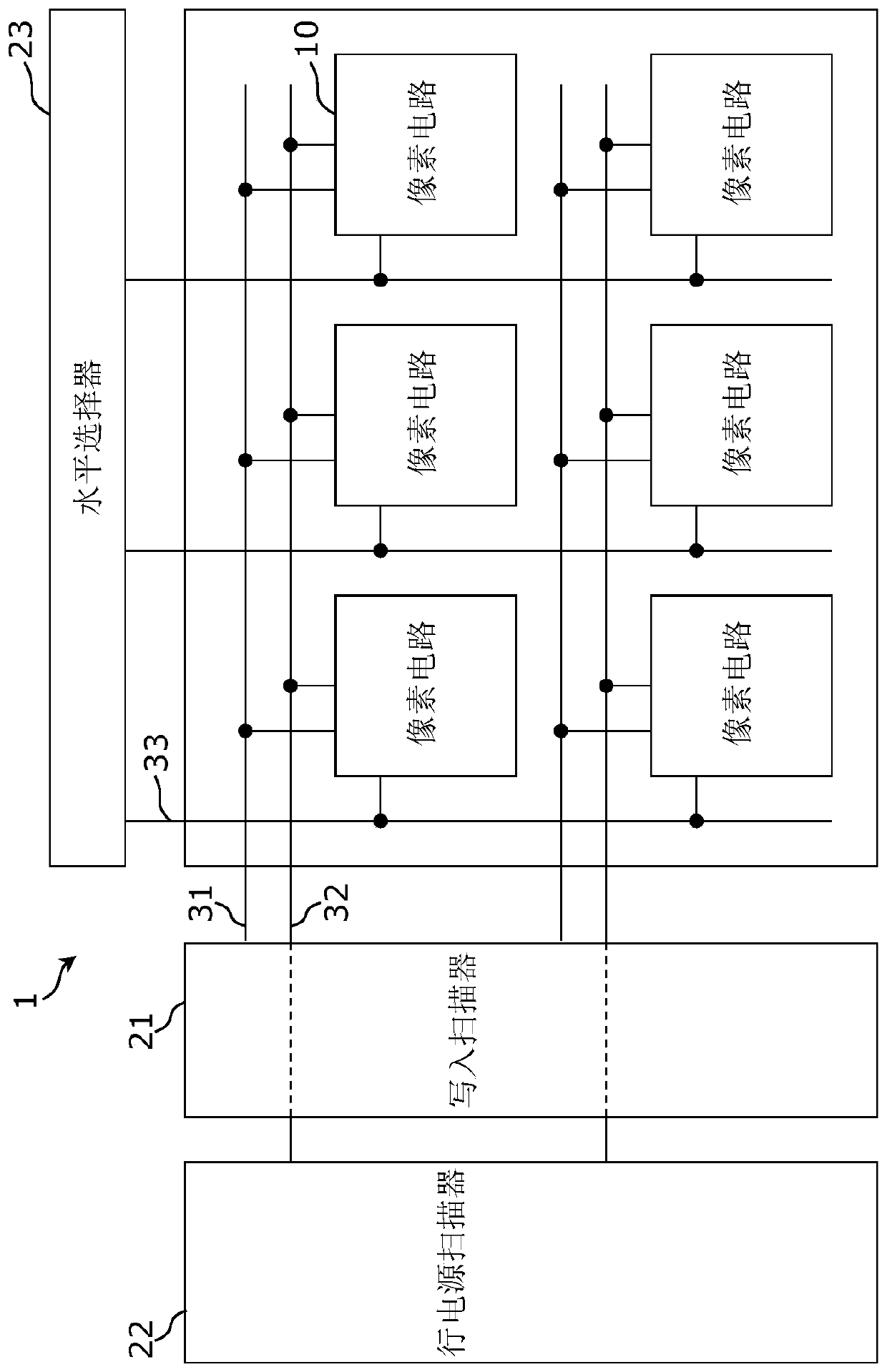
  • Transfer circuit, shift register, gate driver, display panel, and flexible substrate
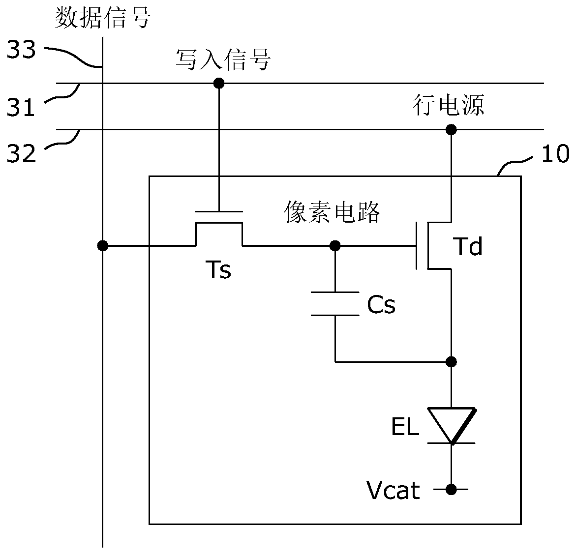
  • Transfer circuit, shift register, gate driver, display panel, and flexible substrate
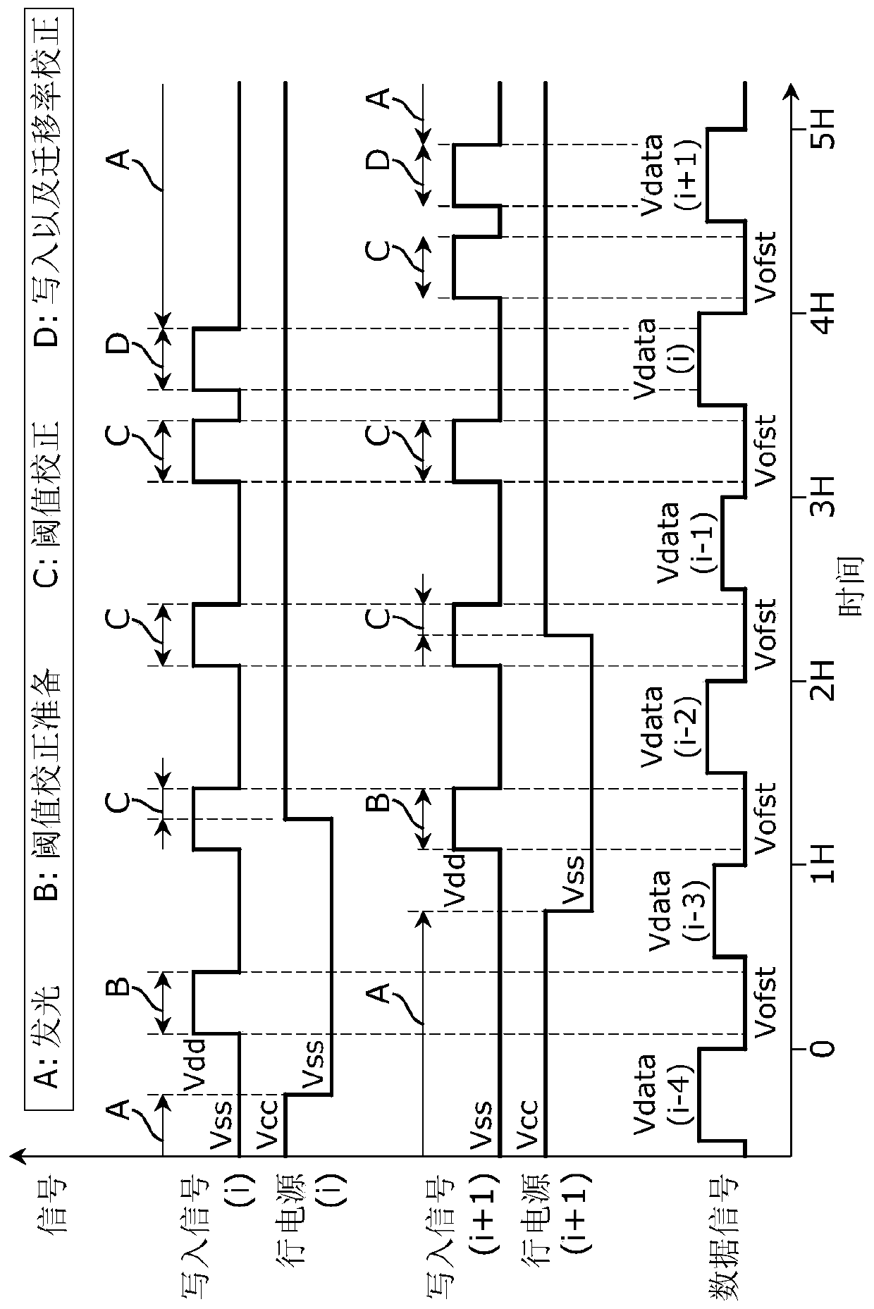
  • Transfer circuit, shift register, gate driver, display panel, and flexible substrate

Examples


Embodiment 1

[0090] Hereinafter, Embodiment 1 of the present invention will be described with reference to the drawings.

[0091] Figure 9 It is a circuit diagram showing an example of the configuration of the transmission circuit according to the first embodiment. exist Figure 9 In , the symbol enclosed in the parentheses of the signal name represents the representative potential of the high level and low level of the signal in terms of the potential of the power supply. Such as Figure 9 As shown, the transmission circuit 200 is constructed as, will Figure 5 The output stabilization circuit 140 of the shown transmission circuit 100 is replaced by the output stabilization circuit 240 . The output stabilization circuit 240 is configured by adding an inverter circuit 250 for outputting an inverted signal of the output signal OUT and a transistor T8 to the output stabilization circuit 140 .

[0092]The inverter circuit 250 is composed of transistors T9, T10, T11, and a capacitor C2, ...

Embodiment 2

[0112] Hereinafter, Embodiment 2 of the present invention will be described with reference to the drawings.

[0113] Figure 13A , Figure 14A It is a circuit diagram showing an example of the structure of the output stabilization circuit which is the main part of the transmission circuit according to the second embodiment.

[0114] Figure 13A The output stabilization circuit 301 is constructed so that Figure 12A to Figure 12D Based on the shown output stabilization circuit, the capacitor C2 is not connected to the output terminal OUT of the transmission circuit, but is connected to the input terminal IN. output stabilization circuit 301, for example, according to Figure 13B The control signals and input signals shown are driven. Figure 13C An example of an operation waveform of the output stabilization circuit 301 is shown. The characteristic of the control signal RST is that it is low level when the potential of the input signal IN and the potential of the output s...


PUM


Abstract

A transfer circuit (200) includes an input circuit (110), a reset circuit (120), an output circuit (130), and an output stabilizer circuit (240), and obtains an input signal at an input terminal (IN),holds the input signal, and outputs the input signal from an output terminal (OUT) as an output signal in synchronization with a clock signal. The output stabilizer circuit (240) includes an invertercircuit (250) and a transistor (T8). The inverter circuit (250) outputs from an output terminal an inverted signal having an inverted polarity of at least one of the input signal and the output signal. The transistor (T8) has a control signal end connected to the output terminal of the inverter circuit (250), a first main signal end connected to a power supply line (Vss1) of the output stabilizercircuit (240), and a second main signal end connected to the output terminal of the transfer circuit.

Description

technical field [0001] The invention relates to a transmission circuit, a shift register, a gate driver, a display panel, and a flexible substrate. Background technique [0002] Conventionally, display devices in which a plurality of pixel circuits are arranged in a matrix have been widely used. In such a display device, a plurality of pixel circuits are sequentially driven row by row using a control signal having a different timing for each row to display an image. Control signals for each row are generated, for example, using a shift register. Patent Document 1 discloses a register circuit usable as a transfer circuit of each stage of such a shift register. [0003] Patent Document 1: Japanese Patent Laid-Open No. 2017-45499 [0004] In the register circuit disclosed in Patent Document 1, the potential of the output signal, which should be a low level potential, may rise slightly. Therefore, in a shift register in which a plurality of such register circuits are connect...

Claims


Application Information

Patent Timeline
Patent Type & Authority Applications(China)
IPC IPC(8): G11C19/28G09G3/20
CPCG11C19/28G09G3/20G09G2310/0286G09G3/3266G09G3/32G09G3/3648
Inventor 山本哲郎
Owner JOLED INC
Learn More