Screen design method and device for OLED (organic light emitting diode) based on optical path matching

A screen design and optical path technology, applied in the field of OLED screen design, can solve problems such as ghosting, low image quality, and blur

Active Publication Date: 2019-07-16
TSINGHUA UNIV +1
View PDF11 Cites 7 Cited by
  • Summary
  • Abstract
  • Description
  • Claims
  • Application Information

AI Technical Summary

Problems solved by technology

[0005] For this reason, this application proposes a screen design method and device based on optical path matching OLED, in order to realize the phase distribution of OLED by adjusting the microstructure of each layer in OLED, so as to solve the periodicity in the OLED screen in the prior art Ghosting and blurring caused by the structure, leading to technical problems of low image quality

Method used


Image

  • Screen design method and device for OLED (organic light emitting diode) based on optical path matching
  • Screen design method and device for OLED (organic light emitting diode) based on optical path matching
  • Screen design method and device for OLED (organic light emitting diode) based on optical path matching

Examples


Embodiment Construction

[0028] The following describes in detail the embodiments of the present application, examples of which are illustrated in the accompanying drawings, wherein the same or similar reference numerals refer to the same or similar elements or elements having the same or similar functions throughout. The embodiments described below with reference to the accompanying drawings are exemplary, and are intended to be used to explain the present application, but should not be construed as a limitation to the present application.

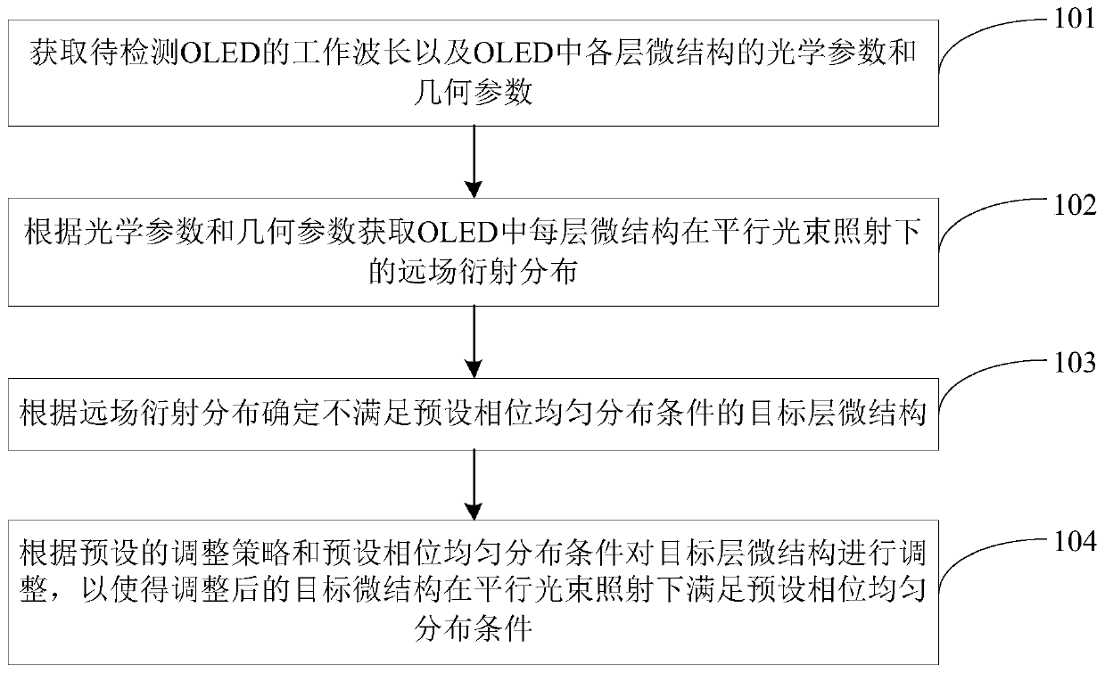
[0029] This application mainly aims at the technical problem of low shooting quality due to the phenomenon of ghosting or blurring due to the periodic structure in the OLED screen during shooting of the OLED screen in the prior art, and proposes an OLED screen based on optical path matching. design method.

[0030] The optical path matching-based OLED screen design method implemented in the present application suppresses the imaging ghost phenomenon by adjusting ...


PUM


Abstract

The invention discloses a screen design method and device for an OLED (organic light emitting diode) based on optical path matching. The screen design method for the OLED based on optical path matching comprises the steps that the working wavelength of the OLED to be detected and optical parameters and geometric parameters of each layer of microstructures are obtained, the far field diffraction distribution of each layer of the microstructures in the OLED under the illumination of parallel beams are obtained according to the optical parameters and the geometric parameters to determine a targetlayer microstructure which does not meet a preset phase uniform distribution condition; the target layer microstructure is adjusted according to a preset adjustment strategy and the preset phase uniform distribution condition so that the adjusted target microstructure meets the preset phase uniform distribution condition under the illumination of the parallel beams. Thus, by adjusting the targetlayer microstructure until the adjusted target layer microstructure meets the phase uniform distribution condition under the illustration of the parallel beams, resulting ghosting and blurring phenomena caused by a periodic structure in an OLED screen when imaging using an under-screen imaging system are suppressed, and imaging quality is significantly improved.

Description

technical field [0001] The present application relates to the technical field of transparent organic light emitting diodes, and in particular, to a screen design method and device based on an OLED with optical path matching. Background technique [0002] With the popularization and development of front cameras on mobile phones and other portable electronic devices, and the continuous improvement of users' taste in the design of electronic devices, how to maximize the screen occupation of the display area while meeting the needs of users to take selfies with the front camera Comparing, making the screen of mobile phones and other portable electronic devices infinitely approaching a full screen has gradually become a problem that people pay attention to. The OLED screen currently used in mobile phones is a multi-layer display device made of transparent materials with a certain transmittance. The optical parameters (refractive index, transmittance) and geometric parameters (thi...

Claims


Application Information

Patent Timeline
IPC IPC(8): G09F9/33
CPCG09F9/33
Inventor 曹良才李儒佳吴佳琛袁石林杨鑫
Owner TSINGHUA UNIV
Why Eureka
Try Eureka