Semiconductor equipment front-end module, semiconductor equipment and wafer processing method
A technology of equipment front-end modules and processing methods, which is applied in semiconductor/solid-state device manufacturing, electrical components, conveyor objects, etc., can solve problems such as bad chips, increased production costs, and decreased product yield, so as to reduce production costs and improve Production yield and the effect of improving cleanliness
- Summary
- Abstract
- Description
- Claims
- Application Information
AI Technical Summary
Problems solved by technology
Method used
Image
Examples
Embodiment 1
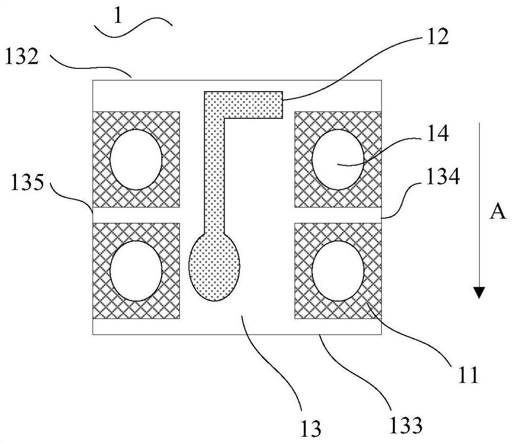
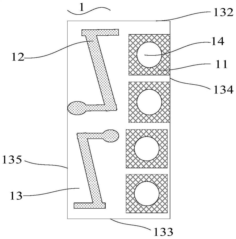
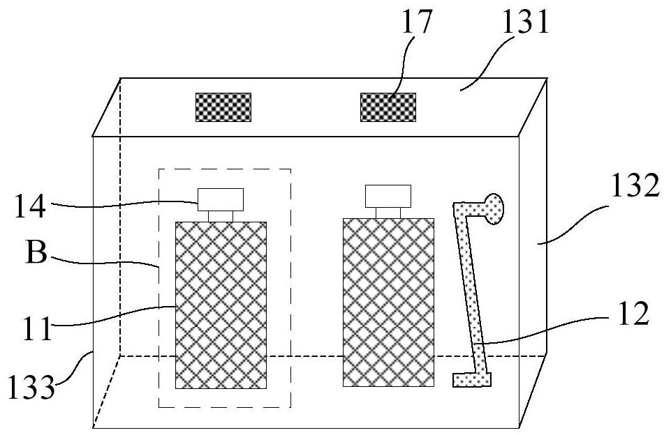
[0060] Such as Figure 1 to Figure 4 As shown, the present invention provides a semiconductor device front-end module 1 . The front-end module 1 of the semiconductor equipment is connected with the reaction chamber module 2 for processing the wafer to be processed. The front-end module 1 of the semiconductor equipment includes a buffer chamber 13, at least two wafer loading ports 11, at least one Mechanical arm 12, box opening device 15 and control device 16. Wherein, the buffer chamber 13 has a top wall 131, a front wall 132, a rear wall 133, a first side wall 134 and a second side wall 135, the top wall 131 is connected to the front wall 132, the rear wall 133, the second side wall 135 The side wall 134 and the second side wall 135 are connected to form a closed space of the buffer chamber 13, wherein the front wall 132 is connected to the reaction chamber module 2 via the load lock module 3; the wafer The loading port 11 is located in the buffer chamber 13 and at least on...
Embodiment 2
[0068] Such as Figure 5As shown, the present invention also provides a semiconductor device for processing the wafer to be processed. The semiconductor equipment includes a reaction chamber module 2 and the front-end module 1 of the semiconductor equipment in Embodiment 1. The front-end module 1 of the semiconductor equipment is connected to the reaction chamber module 2 via the load-lock module 3 for The wafer to be processed is transferred into the reaction chamber module 2 , and the processed wafer is removed from the reaction chamber module 2 . The reaction chamber module 2 includes at least one reaction chamber 21 . It should be noted that, in the case of only one reaction chamber, the reaction chamber module 2 can be regarded as one reaction chamber 21 . Of course, in order to make full use of the space in the clean room, generally there are multiple reaction chambers 21, such as 3, 4, 5 or even more. According to different needs and different equipment structures, t...
Embodiment 3
[0072] see Figure 7 , the present invention also provides a wafer processing method, the wafer processing method is carried out using the semiconductor equipment front-end module 1 as in Embodiment 1, and the wafer processing method includes:
[0073] Step S1, loading at least two front-end wafer cassettes 14 loaded with wafers to be processed on the wafer loading port 11 of the semiconductor equipment front-end module 1, wherein the semiconductor equipment front-end module 1 is used to use different described The FOUP cassettes 14 are placed in the working state and the standby state respectively, and when one of the FOUP cassettes 14 is in the working state, the other FOUPs 14 are in the standby state, so as to deal with different The wafers to be processed in the front open wafer cassette 14 are sequentially processed;
[0074] Step S2, opening the lid of the FOUP 14 in the working state, and closing the lid of the FOUP 14 in the standby state;
[0075] In step S3, the w...
PUM
 Abstract
Description
Claims
Application Information
 - R&D Engineer
- R&D Manager
- IP Professional
- Industry Leading Data Capabilities
- Powerful AI technology
- Patent DNA Extraction
Browse by: Latest US Patents, China's latest patents, Technical Efficacy Thesaurus, Application Domain, Technology Topic, Popular Technical Reports.
© 2024 PatSnap. All rights reserved.Legal|Privacy policy|Modern Slavery Act Transparency Statement|Sitemap|About US| Contact US: help@patsnap.com


