
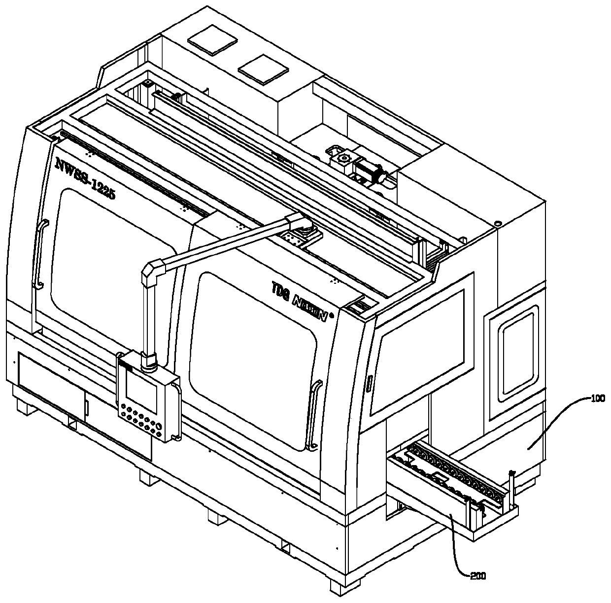
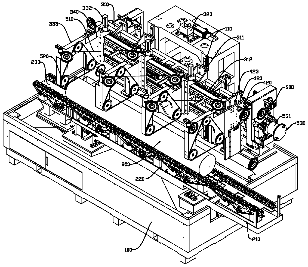
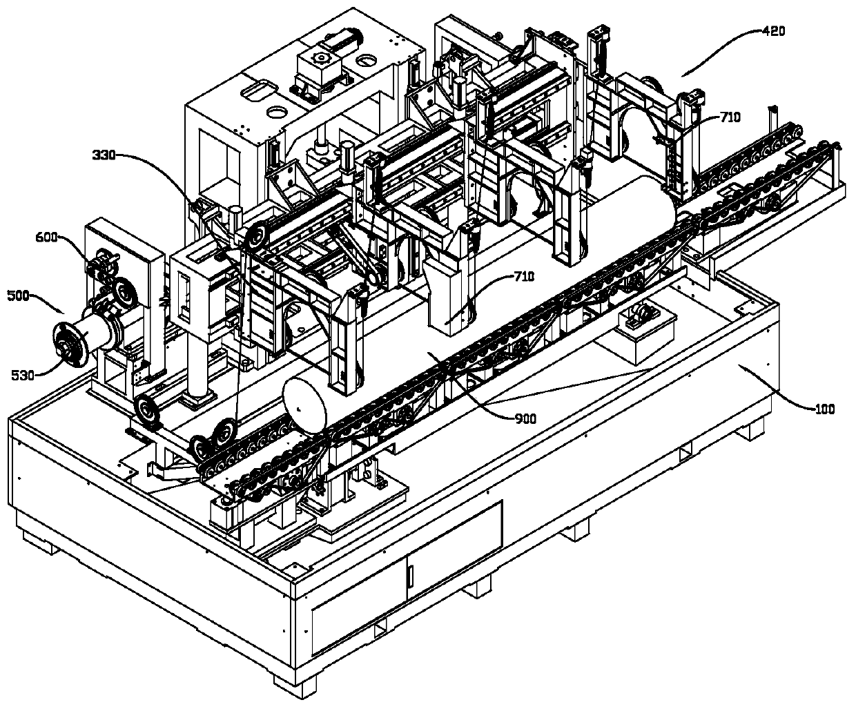
Cutting machine of multi-section semiconductor crystal rod

A semiconductor, multi-segment technology, applied in the direction of fine working equipment, stone processing equipment, manufacturing tools, etc., can solve problems such as low efficiency, reduced utilization rate of ingot segments, and missing corners of ingot segments

Pending Publication Date: 2019-06-14
TDG NISSIN PRECISION MACHINERY CO LTD
View PDF0 Cites 5 Cited by
  • Summary
  • Abstract
  • Description
  • Claims
  • Application Information

AI Technical Summary

Problems solved by technology

[0003] However, there are still deficiencies in current semiconductor ingot cutting machines. For example, the existing semiconductor ingot cutting machines often have a single cutting function and cannot adapt to the ingot cutting processing of various requirements; in addition, the existing semiconductor ingot cutting machines Before the workpiece is processed, it often lacks the leveling function of the workpiece, resulting in that after the semiconductor crystal rod is cut off, due to the uniformity of the semiconductor crystal rod itself, there is a gap between the truncated surface at both ends and the longitudinal center axis of the semiconductor crystal rod itself. Not vertical enough
And the error is passed into the subsequent ingot rounding, so that the effective utilization rate of the semiconductor ingot is greatly reduced
At the same time, in the process of cutting the crystal ingot and sampling the existing semiconductor ingot cutting machine, when it is necessary to intercept multiple test samples at one semiconductor ingot cutoff, it often needs to be cut through multiple cuts. The way the process is lengthy and inefficient
[0004] Finally, in the existing semiconductor crystal rod cutting device, adjacent crystal rod segments often collide with each other during the transfer process of the crystal rod segments, resulting in missing corners between the truncated surfaces of the crystal rod segments and reducing the utilization of the crystal rod segments. Rate

Method used


Image

  • Cutting machine of multi-section semiconductor crystal rod
  • Cutting machine of multi-section semiconductor crystal rod
  • Cutting machine of multi-section semiconductor crystal rod

Examples


Embodiment Construction

[0045] Embodiments of the present invention are described in detail below, examples of which are shown in the drawings, wherein the same or similar reference numerals denote the same or similar elements or elements having the same or similar functions throughout. The embodiments described below by referring to the figures are exemplary only for explaining the present invention and should not be construed as limiting the present invention.

[0046]In describing the present invention, it should be understood that the terms "center", "longitudinal", "transverse", "length", "width", "thickness", "upper", "lower", "front", " Orientation indicated by rear, left, right, vertical, horizontal, top, bottom, inside, outside, clockwise, counterclockwise, etc. The positional relationship is based on the orientation or positional relationship shown in the drawings, which is only for the convenience of describing the present invention and simplifying the description, rather than indicating o...


PUM


Abstract

The invention discloses a cutting machine of a multi-section semiconductor crystal rod. The cutting machine comprises a base, a material conveying device, a single-section cutting device, a multi-section cutting device and a routing system, wherein sample sheets at cutting parts can be cut and intercepted synchronously from the semiconductor crystal rod in real time by the single-section cutting device and the multi-section cutting device; in comparison with current separate operations of interception and sampling, the cutting machine has the advantages of simple operations and high processingefficiency; and the cutting machine disclosed by the invention is also equipped with a center alignment device which can be used to adjust a horizontal degree of the semiconductor crystal rod locatedon the material conveying device, so a perpendicular degree between the cross section of the semiconductor crystal rod and a center axis of the cutting machine can be increased effectively, and a utilization rate of crystal rod sections in subsequent rounding processing can be increased.

Description

technical field [0001] The invention relates to a semiconductor crystal rod cutting machine, in particular to a multi-stage semiconductor crystal rod cutting machine. Background technique [0002] Wire cutting technology is currently the world's most advanced semiconductor ingot cutting machine. Its principle is to process workpieces (such as single crystal silicon rods, sapphire or other semiconductor brittle and hard materials) through reciprocating friction of high-speed diamond wires. The surface is rubbed to cut a long semiconductor ingot into a short ingot, so as to facilitate the next step of rounding the ingot. During the cutting process of the semiconductor ingot, the diamond wire is guided by the guide wheel to form a wire net on the main wire roller, and the workpiece to be processed is fed by the rise and fall of the worktable, under the action of the pressure pump , the cooling water automatic spraying device installed on the equipment sprays the cooling water ...

Claims


Application Information

Patent Timeline
Patent Type & Authority Applications(China)
IPC IPC(8): B28D5/04B28D5/00
Inventor 卢建伟苏静洪张峰裴忠李鑫潘雪明曹奇峰
Owner TDG NISSIN PRECISION MACHINERY CO LTD
Learn More