Semiconductor integrated circuit test device
A technology for integrated circuits and testing devices, applied in the field of semiconductor integrated circuit testing devices, can solve the problems of unfavorable cost reduction in efficiency, high-cost RF circuits, and poor prices.
- Summary
- Abstract
- Description
- Claims
- Application Information
AI Technical Summary
Problems solved by technology
Method used
Image

Examples
no. 1 example
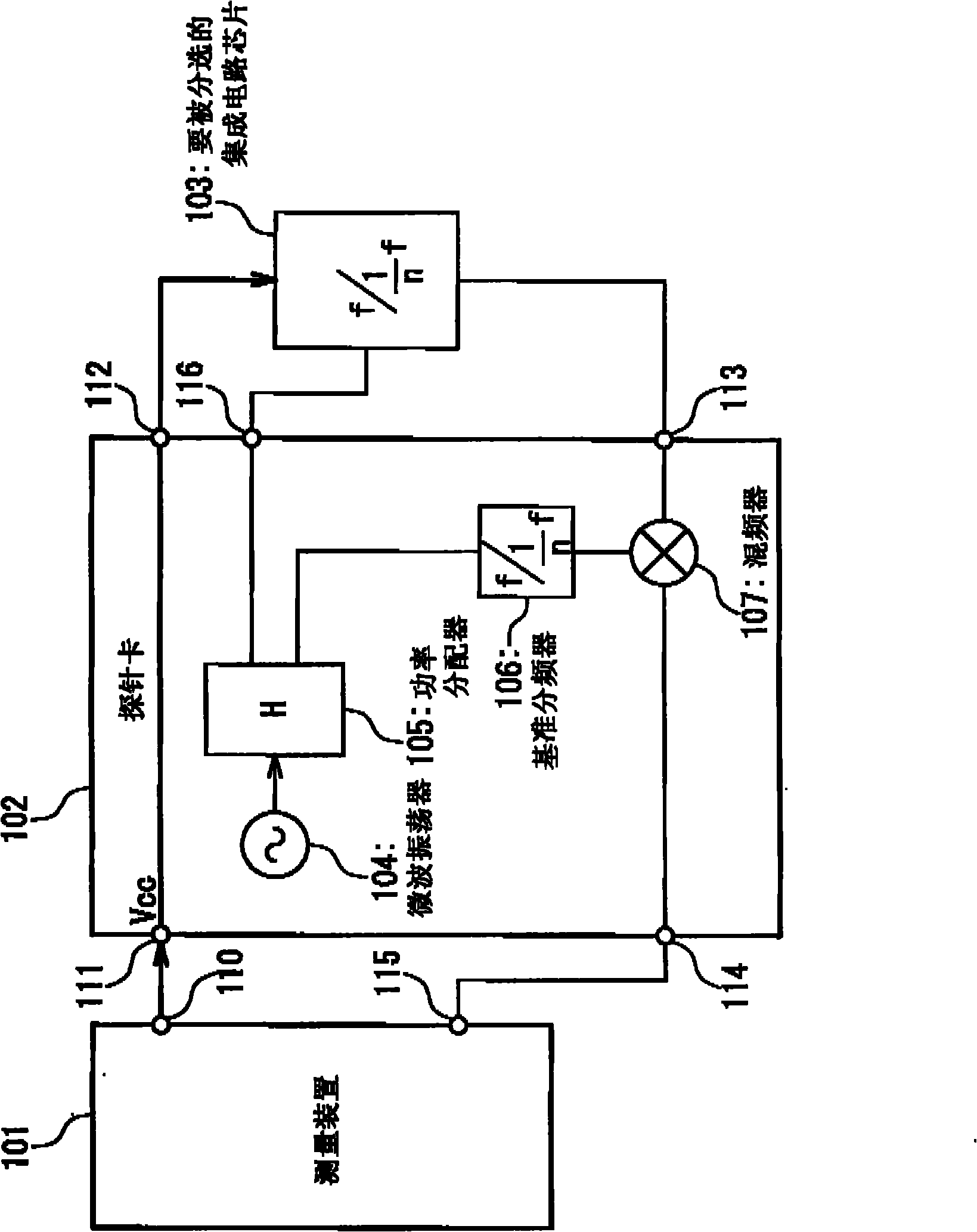
[0037] image 3 is an overall view for describing the configuration of the semiconductor integrated circuit testing device in the first embodiment according to the present invention. The semiconductor integrated circuit testing apparatus includes an IC tester 10 and a probe card 20-1.
[0038] First, the semiconductor integrated circuit 40-1 in this embodiment will be described. It is assumed that the prescaler 41 to be measured having a PLL therein is connected to the semiconductor integrated circuit testing apparatus in this embodiment. In other words, the semiconductor integrated circuit testing apparatus in this embodiment is intended to test the semiconductor integrated circuit 40-1 having the configuration described below. That is, the semiconductor integrated circuit 40-1 in this embodiment includes a plurality of input / output parts, a frequency divider 41 as a prescaler to be tested, a VCO 42, an LPF 43, and a PFD (Phase Frequency Detector) 44. Here, the PFD44, LPF4...
no. 2 example
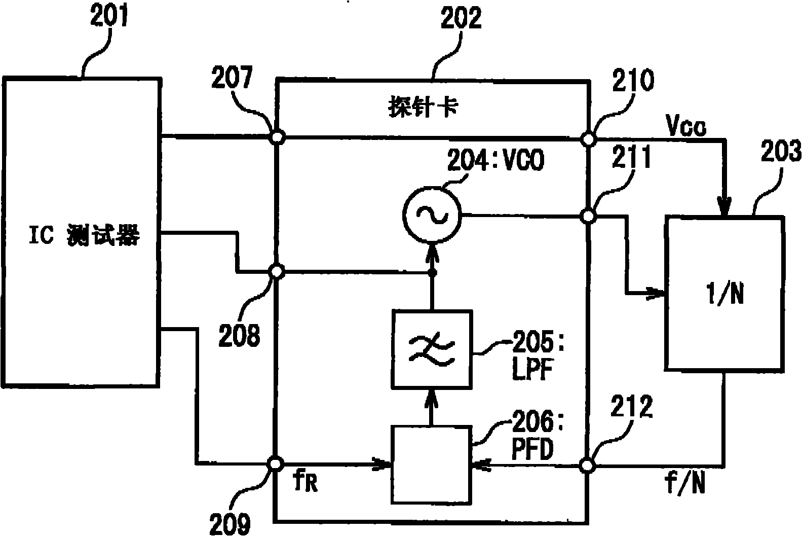
[0060] Figure 7 is an overall view for describing the configuration of the semiconductor integrated circuit testing device in the second embodiment according to the present invention. The semiconductor integrated circuit testing apparatus includes an IC tester 10 and a probe card 20-2.
[0061] This embodiment differs from the first embodiment of the present invention in the positions of PFD28 and LPF27. That is, in the first embodiment of the present invention, the prescaler of the semiconductor integrated circuit 40-1 to be measured includes PFD44 and LPF43. However, in the present embodiment, probe card 20-2 includes PFD28 and LPF27 instead.
[0062] This means that in the present embodiment, even when the prescaler of the semiconductor integrated circuit 40-2 to be measured does not include a PLL circuit, the semiconductor integrated circuit testing method can be performed as in the first embodiment of the present invention.
[0063] First, the semiconductor integrated...
no. 3 example
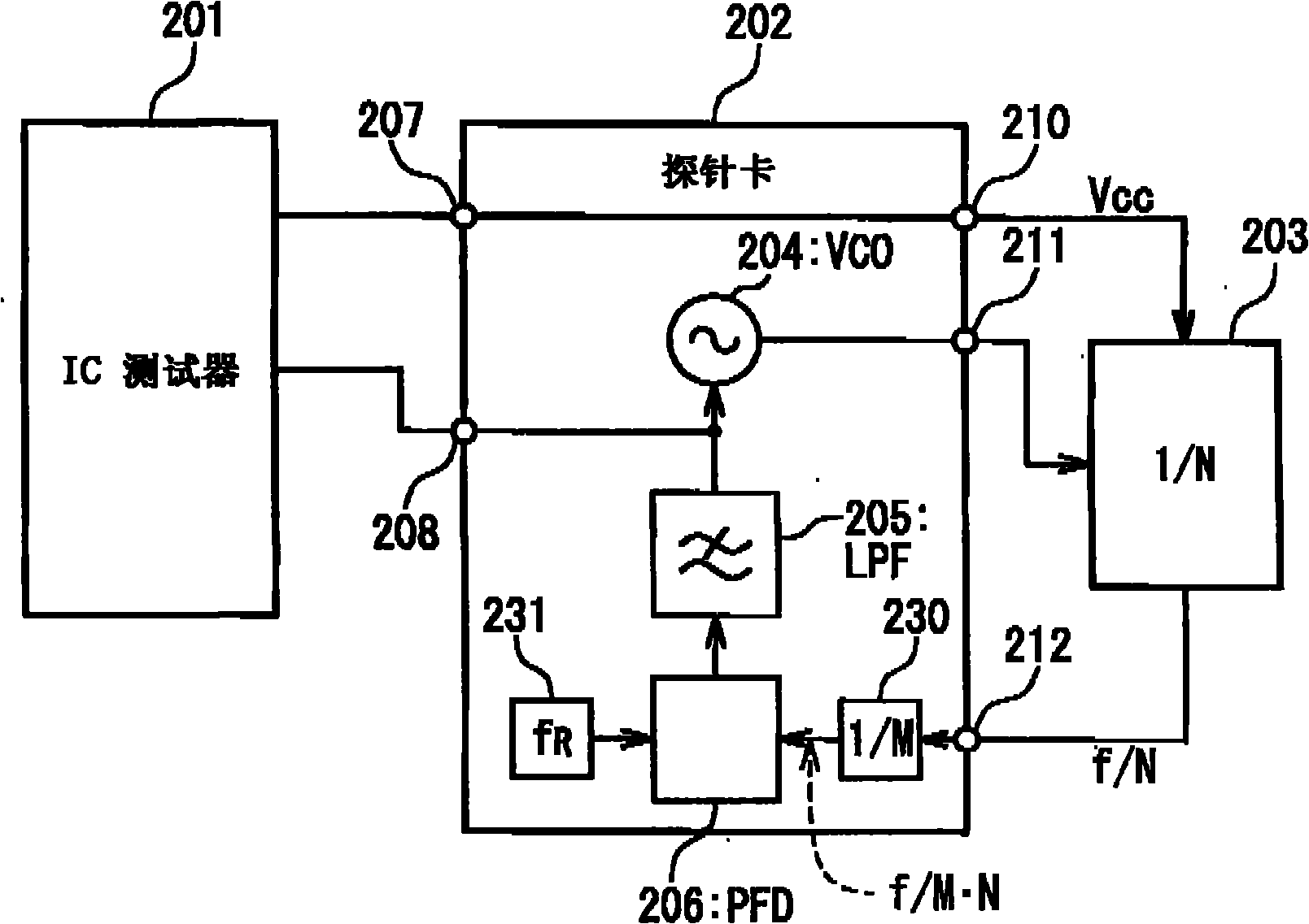
[0069] Figure 8A is an overall view for describing the configuration of a semiconductor integrated circuit testing device in a third embodiment according to the present invention. This semiconductor integrated circuit testing apparatus includes an IC tester 10 and a probe card 20-3.
[0070] The present embodiment differs from the second embodiment of the present invention mainly in the connection between the outputs of the two frequency dividers 41, 25 in the circuits of the probe cards 20-2, 20-3 and the inputs of the IC tester 10. part. This section includes a phase comparison circuit section that compares phases of two signals with each other and outputs a signal based on the phase difference; and a conversion circuit that converts the output signal of the phase comparison circuit section into a DC voltage. That is, the probe card 20-2 in the second embodiment of the present invention includes PFD28 and LPF27 as phase comparison circuit parts, and the probe card 20-3 in...
PUM
 Abstract
Description
Claims
Application Information
 - Generate Ideas
- Intellectual Property
- Life Sciences
- Materials
- Tech Scout
- Unparalleled Data Quality
- Higher Quality Content
- 60% Fewer Hallucinations
Browse by: Latest US Patents, China's latest patents, Technical Efficacy Thesaurus, Application Domain, Technology Topic, Popular Technical Reports.
© 2025 PatSnap. All rights reserved.Legal|Privacy policy|Modern Slavery Act Transparency Statement|Sitemap|About US| Contact US: help@patsnap.com