A Method of Reducing Buried Resistor Error

A technology of resistance and error, which is applied in the field of circuit board processing and manufacturing, can solve the problems of large resistance error, achieve good uniformity, good compatibility, and realize the effect of large-scale promotion and application

Active Publication Date: 2021-07-02
UNIV OF ELECTRONICS SCI & TECH OF CHINA
View PDF0 Cites 0 Cited by
  • Summary
  • Abstract
  • Description
  • Claims
  • Application Information

AI Technical Summary

Problems solved by technology

[0005] Aiming at the problems that the existing embedded resistors used in printed circuit boards have large resistance value errors and the stability of embedded resistors between different batches is poor in terms of their functional values, the invention provides a method to reduce the embedded resistors. The method of resistance resistance error

Method used


Image

  • A Method of Reducing Buried Resistor Error
  • A Method of Reducing Buried Resistor Error

Examples


Embodiment

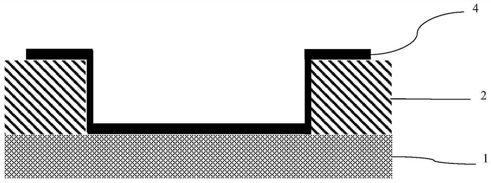
[0028] This embodiment provides a method for reducing the resistance error of the embedded resistor, which specifically includes the following steps:

[0029] Step 1: Make the conductive traces of the PCB:

[0030] Use the epoxy resin double-sided copper-clad laminate with a dielectric layer thickness of 100 μm and a copper thickness of 12 μm produced by Shengyi Company as the inner layer plate, and paste a photoresist layer on the surface of the conductor layer 2 of the double-sided copper-clad laminate, using wet film coating or Dry film is pressed, then exposed and developed to realize the transfer of conductive patterns. Specifically, film exposure method or laser direct imaging method can be used, and then acidic etching potion or alkaline etching potion is used to remove the excess conductor layer 2, and peel off the covering on the target. The photoresist layer of the conductive circuit to complete the production of the conductive circuit;

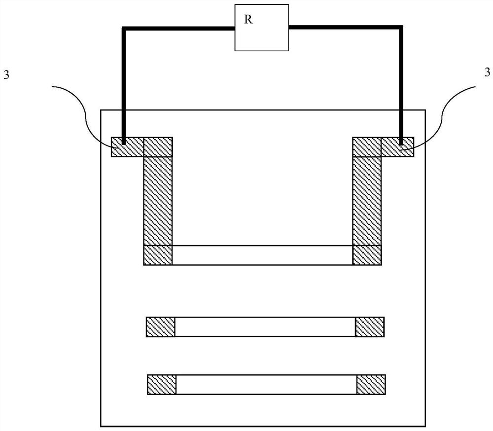
[0031] Step 2: Design of Em...


PUM


Abstract

The invention discloses a method for reducing the resistance value error of an embedded resistor, which belongs to the technical field of circuit board processing and manufacturing. In the invention, a resistive layer deposition area and a resistance monitoring device access area are simultaneously formed on the inner circuit of the printed circuit board. Then, when the resistance layer is deposited to make a resistor, the resistance value of the resistance layer is monitored by a resistance monitoring device to reach a standard resistance value. The invention can solve the problems of poor resistance stability in the manufacturing process of the existing embedded resistor and the resistance value of the embedded resistor does not meet the design requirements due to sensitive process. Using the method of the present invention can make the square resistance of the embedded resistors prepared between different batches basically consistent, with good uniformity, and the relative error with the standard resistance value is very small, which meets the error standard of the first-class device. At the same time, the method The invention has good compatibility with the manufacturing method of the existing embedded resistors, can realize the embedding of large resistance resistors, is beneficial to circuit design, and can realize large-scale popularization and application in the printed circuit board industry.

Description

technical field [0001] The invention belongs to the technical field of circuit board processing and manufacturing, and in particular relates to a method for reducing the resistance value error of an embedded resistor. Background technique [0002] The miniaturization, integration and multifunctionalization of electronic products are the most important driving force for the development of the electronic industry. PCB (Printed Circuit Board, printed circuit board) is the most important assembly platform for electronic products. While electronic products are developing in the direction of miniaturization, multi-function, high reliability, integration, and portability, printed circuit boards are also facing challenges. Unprecedented challenges. For a long time, various components and subsystems are assembled on the surface of the printed circuit board, which inevitably leads to the complexity of the circuit layout and system of the printed circuit board. Since most of the comp...

Claims


Application Information

Patent Timeline
Patent Type & Authority Patents(China)
IPC IPC(8): H01C17/235H01C17/22H01C17/075H01C17/065
Inventor 周国云苟雪萍张秀梅何为王守绪陈苑明洪延王翀杨文君
Owner UNIV OF ELECTRONICS SCI & TECH OF CHINA
Why Eureka
Try Eureka