
Chip-on-film package flexible circuit board, flexible circuit board and manufacturing method thereof

A flexible circuit board and flexible display technology, which is applied to printed circuit components, printed circuits connected with non-printed electrical components, and electrically connected printed components, can solve problems such as short circuit of flexible circuit boards and easy residual metal shavings. To achieve the effect of avoiding short circuit and reducing the possibility of foreign matter remaining

Active Publication Date: 2020-02-21
XIAMEN TIANMA MICRO ELECTRONICS
View PDF4 Cites 0 Cited by
  • Summary
  • Abstract
  • Description
  • Claims
  • Application Information

AI Technical Summary

Problems solved by technology

[0004] The embodiment of the present application provides a chip-on-chip packaged flexible circuit board, a flexible circuit board and a manufacturing method thereof, which are used to solve the technical problem in the prior art that cutting a flexible circuit board tends to leave metal shavings and cause a short circuit of the flexible circuit board

Method used


Image

  • Chip-on-film package flexible circuit board, flexible circuit board and manufacturing method thereof
  • Chip-on-film package flexible circuit board, flexible circuit board and manufacturing method thereof
  • Chip-on-film package flexible circuit board, flexible circuit board and manufacturing method thereof

Examples


Embodiment Construction

[0027] In order to make the purpose, technical solutions and advantages of the present invention clearer, the technical solutions in the embodiments of the present application will be clearly and completely described below in conjunction with the drawings in the embodiments of the present application. It should be understood that the preferred embodiments described below are only used to illustrate and explain the present invention, not to limit the present invention. And in the case of no conflict, the embodiments in the present application and the features in the embodiments can be combined with each other. It should be noted that the length and shape of the output pads in the drawings do not reflect the real scale, and the purpose is only to illustrate the content of the present invention. And the same or similar reference numerals represent the same or similar elements or elements having the same or similar functions throughout.

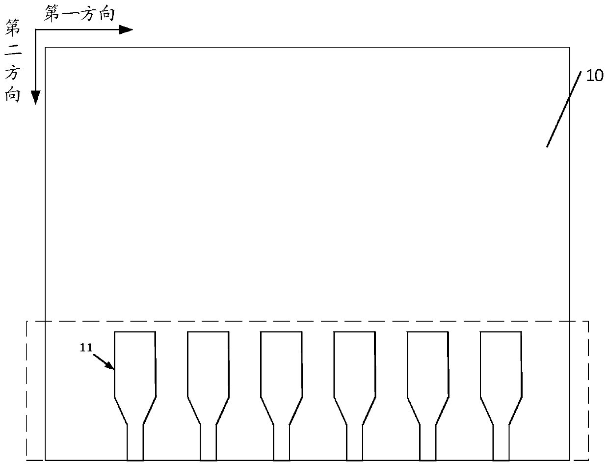
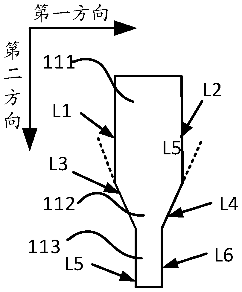
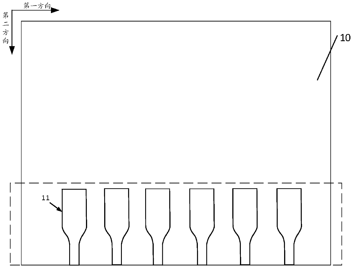
[0028] See figure 1 , the embodiment of ...


PUM


Abstract

The invention discloses a chip-on-film package flexible circuit board, a flexible circuit board and a manufacturing method thereof to solve the technical problem in the prior art that it is likely toleave metal chips and thus cause a short circuit of the flexible circuit board to cut the flexible circuit board. The flexible circuit board includes: a flexible display substrate, and a plurality ofoutput pads arranged in a first direction and disposed on a side of the flexible display substrate, wherein each output pad comprises a first main portion, a first sub portion and a second sub portion; the first end portion of the first sub portion is connected to the first main portion; the second end portion of the first sub portion is connected to the second sub portion; in the first direction,the width of the first main body portion is greater than the width of the first sub portion, and the width of the first sub portion is greater than the width of the second sub portion.

Description

technical field [0001] The invention relates to the technical field of circuit connectors, in particular to a chip-on-film packaging flexible circuit board, a flexible circuit board and a manufacturing method thereof. Background technique [0002] A flexible printed circuit board (Flexible Printed Circuit Board, FPC) is a printed circuit made of a flexible substrate, which can be bent and folded freely, so as to achieve the integration of component assembly and wire connection. Chip On Film (COF) packaged flexible circuit board is used as an integral part of FPC to bind components such as chips. Specifically, a plurality of output pads are arranged on the bonding area of ​​the COF packaged flexible circuit board for Bind components such as chips. [0003] The COF packaged flexible circuit board needs to cut the bonding area before bonding. At present, the interval between two adjacent output pads is narrow, so that foreign matter such as metal shavings generated by the cutt...

Claims


Application Information

Patent Timeline
Patent Type & Authority Patents(China)
IPC IPC(8): H05K1/11H05K1/18H05K3/40
Inventor 庄知龙黄建才许育民
Owner XIAMEN TIANMA MICRO ELECTRONICS
Learn More