OLED display panel and OLED display device

A display panel and sub-display area technology, which is applied in the direction of electrical components, electrical solid devices, circuits, etc., can solve the problems of high cost, uneven brightness, and complicated design and manufacturing process of double-layer SD structure, so as to achieve production cost reduction, production Simplify the process and improve the effect of uneven light emission

Active Publication Date: 2019-05-28
WUHAN CHINA STAR OPTOELECTRONICS SEMICON DISPLAY TECH CO LTD
View PDF4 Cites 2 Cited by
  • Summary
  • Abstract
  • Description
  • Claims
  • Application Information

AI Technical Summary

Problems solved by technology

However, the design of the double-layer SD structure is restricted by the disadvantages of complex manufacturing process and high cost.
[0005] Therefore, there is an urgent need for a novel OLED display panel to overcome the defects of uneven brightness of the existing OLED display panels

Method used


Image

  • OLED display panel and OLED display device
  • OLED display panel and OLED display device
  • OLED display panel and OLED display device

Examples


Embodiment Construction

[0022] The specific implementation manners of the OLED display panel and the OLED display device provided by the present invention will be described in detail below with reference to the accompanying drawings.

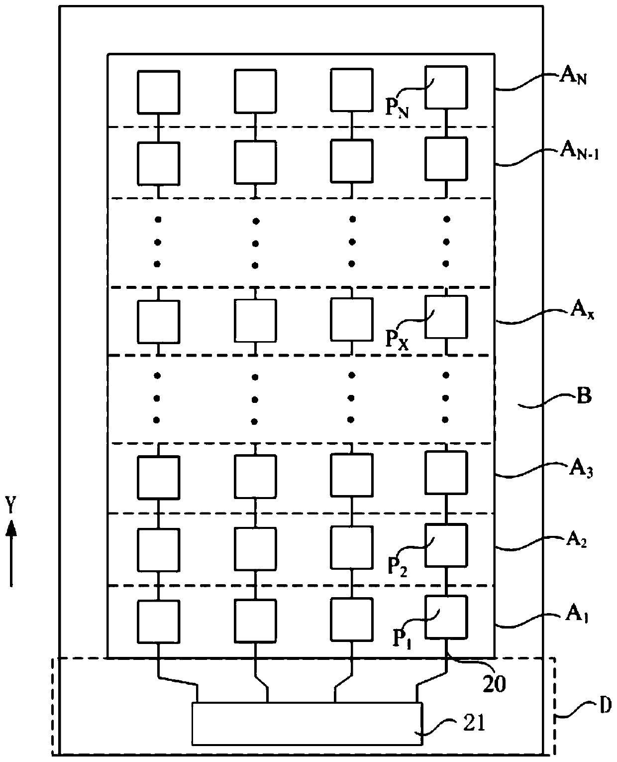
[0023] figure 2 It is a structural schematic diagram of an embodiment of the OLED display panel of the present invention. see figure 2 , The OLED display panel of the present invention includes a driving region D and a plurality of sub-display regions, and the sub-display regions are sequentially arranged along a direction away from the driving region D. For the convenience of description, in this paper, along the direction away from the driving area D (such as figure 2 The Y direction shown in ) defines the sub-display area as the first sub-display area A in turn 1 , the second sub-display area A 2 ...the Xth sub-display area A X ...Nth sub-display area A N , where X and N are natural numbers, that is, the first sub-display area A 1 The distance to the drivi...


PUM


Abstract

The invention discloses an OLED display panel and an OLED display device. The OLED display panel and the OLED display device have the advantages that the OLED display panel is divided into a pluralityof sub-display areas, the storage capacitance is large and the working current is relatively large in the sub-display area far away from one side of a driving area, so that the small working currentat one side, far away from the driving area, of the traditional OLED display panel can be compensated and the non-uniformity of luminescence is improved. Compared with a double-layer SD structure design, the OLED display panel and the OLED display device have the advantages that the manufacturing process is simplified, the production cost is reduced, and the wide applicability of the display device can be improved.

Description

technical field [0001] The invention relates to the display field, in particular to an OLED display panel and an OLED display device. Background technique [0002] In the field of display technology, flat panel display devices such as Liquid Crystal Display (LCD) and Organic Light Emitting Diode (OLED) have gradually replaced cathode line tube displays. Among them, OLED display panels gradually gain the upper hand due to their unique advantages such as low power consumption, high saturation, fast response time and wide viewing angle, and will have broad application space in vehicles, mobile phones, tablets, computers and TV products in the future. [0003] The mainstream driving method of OLED display panels is current drive, and the working current is transmitted from the lower frame of the display panel through the source / drain (SD: Source / Drain). Because the source and drain itself have a certain resistance, there is a voltage drop (IR Drop) in signal transmission. ) phe...

Claims


Application Information

Patent Timeline
Patent Type & Authority Applications(China)
IPC IPC(8): H01L27/32
Inventor 方亮丁玎
Owner WUHAN CHINA STAR OPTOELECTRONICS SEMICON DISPLAY TECH CO LTD
Why Eureka
Try Eureka