Method and apparatus for testing a thin film transistor panel

A technology for transistor substrates and thin film transistors, which is applied in the direction of measuring electricity, measuring devices, measuring electrical variables, etc., and can solve problems such as distortion, signal attenuation, and cost increase.

Inactive Publication Date: 2019-05-28
CENT TECH CORP
View PDF11 Cites 1 Cited by
  • Summary
  • Abstract
  • Description
  • Claims
  • Application Information

AI Technical Summary

Problems solved by technology

[0004] The above method of non-contact signal transmission is usually carried out by capacitive coupling. However, the process of capacitive coupling is easy to attenuate the signal. difficulty
In addition, this non-contact detection method through capacitive coupling is generally only suitable for testing in the display area, and the testing range is limited
For some circuits configured on the periphery of the display area such as the driver IC circuit (Gate drive on array, GOA or Gate drive on panel, GOP), it is usually necessary to wait until the functional test after assembly before performing quality verification. If the TFT substrate If there are any defects in the driver IC circuit, if it cannot be detected and repaired in time after the circuit is manufactured, the repair process after assembly will be more complicated, and the cost will be relatively higher.
The above problems constitute insufficient test quality (identification of defects) and increased rework costs, all of which have room for improvement

Method used


Image

  • Method and apparatus for testing a thin film transistor panel
  • Method and apparatus for testing a thin film transistor panel
  • Method and apparatus for testing a thin film transistor panel

Examples


Embodiment

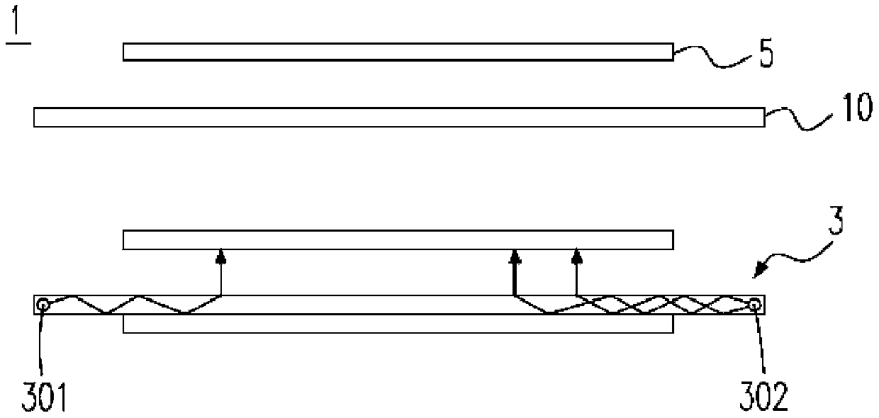
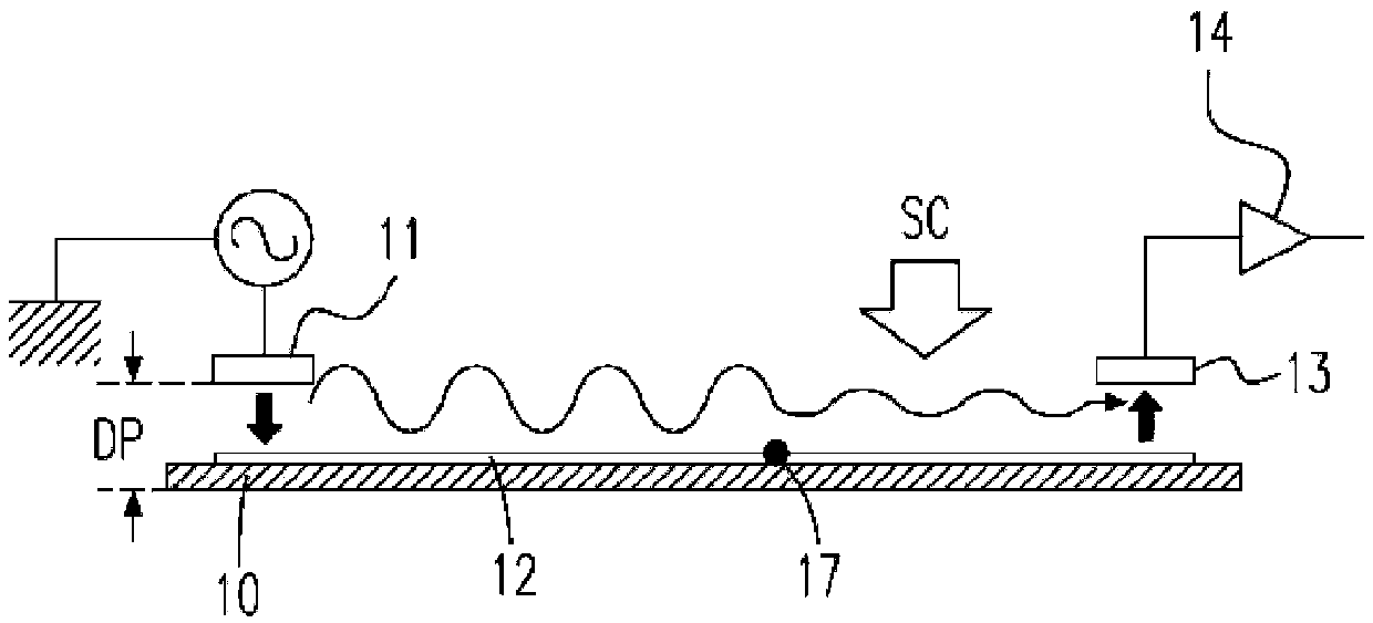
[0031] 1. A method for detecting a thin film transistor substrate, wherein the thin film transistor substrate includes at least one display area and a peripheral area surrounding the display area, the peripheral area has a plurality of function test signal input pads, the method Include:

[0032] Provide multiple probes and a sensing unit;

[0033] respectively disposing the plurality of probes on the plurality of functional test signal input pads to apply a set of test electrical signals to the plurality of functional test signal input pads; and

[0034] The sensing unit is arranged at a sensing position adjacent to an edge of the display area, and sequentially receives sensing signals along the edge in a non-contact manner.

[0035] 2. The method of embodiment 1, wherein the display area has a first display side and a second display side, the peripheral area has a first peripheral side and a second peripheral side, the first display side and the first peripheral side belon...


PUM


Abstract

A method for testing a thin film transistor panel is provided. The thin film transistor panel includes at least a display area and a peripheral area surrounding the display area, and the peripheral area has a plurality of functional testing signal input pads. The method includes providing a plurality of probes and a sensing unit; disposing the plurality of probes at the plurality of functional testing signal input pads to input a group of electrical signals into the pads respectively; and disposing the sensing unit at a sensing position near an edge of the display area and receiving sensing signals via a non-contact method along the edge.

Description

technical field [0001] The invention relates to a detection and detection equipment, in particular to a method for detecting a thin film transistor substrate and a detection device using the method. Background technique [0002] Typical thin film transistor (Thin film transistor, TFT) liquid crystal display devices, such as Figure 1A As shown in the TFT liquid crystal display device 1 in , it is basically composed of a backlight module 3 behind, a CF substrate 5 with a color filter (Color filter, CF) sheet in front, and a TFT substrate 10 in the middle. . The light-emitting components 301 / 301 at both ends of the backlight module 3 can emit light in different directions at the same time, and after reflection and refraction, they become multiple parallel light rays that face upward together and pass through the TFT substrate 10 and the CF substrate 5 in sequence. The TFT substrate 10 is formed on a glass substrate by multi-layer processing to form horizontally and vertically...

Claims


Application Information

Patent Timeline
Patent Type & Authority Applications(China)
IPC IPC(8): G09G3/00G02F1/13
CPCG01R31/282G09G3/006
Inventor 庄文忠
Owner CENT TECH CORP
Why Eureka
Try Eureka