Transistor and manufacturing method of terminal structure thereof

A manufacturing method and terminal structure technology, which is applied in semiconductor/solid-state device manufacturing, semiconductor devices, electrical components, etc., can solve the problems of affecting the operating frequency of the device and consuming a lot of time, so as to improve the operating frequency, reduce the junction capacitance, and achieve durability. The effect of pressure performance

Inactive Publication Date: 2019-05-21
泉州臻美智能科技有限公司
View PDF0 Cites 0 Cited by
  • Summary
  • Abstract
  • Description
  • Claims
  • Application Information

AI Technical Summary

Problems solved by technology

Due to the large area of ​​the JTE junction terminal, for high-voltage devices, the longer the lateral length of the JTE structure, the larger the source-drain capacitance of the device will affect the operating frequency of the device.
In addition, the production of JTE structure will consume a lot of time

Method used


Image

  • Transistor and manufacturing method of terminal structure thereof
  • Transistor and manufacturing method of terminal structure thereof
  • Transistor and manufacturing method of terminal structure thereof

Examples


Embodiment Construction

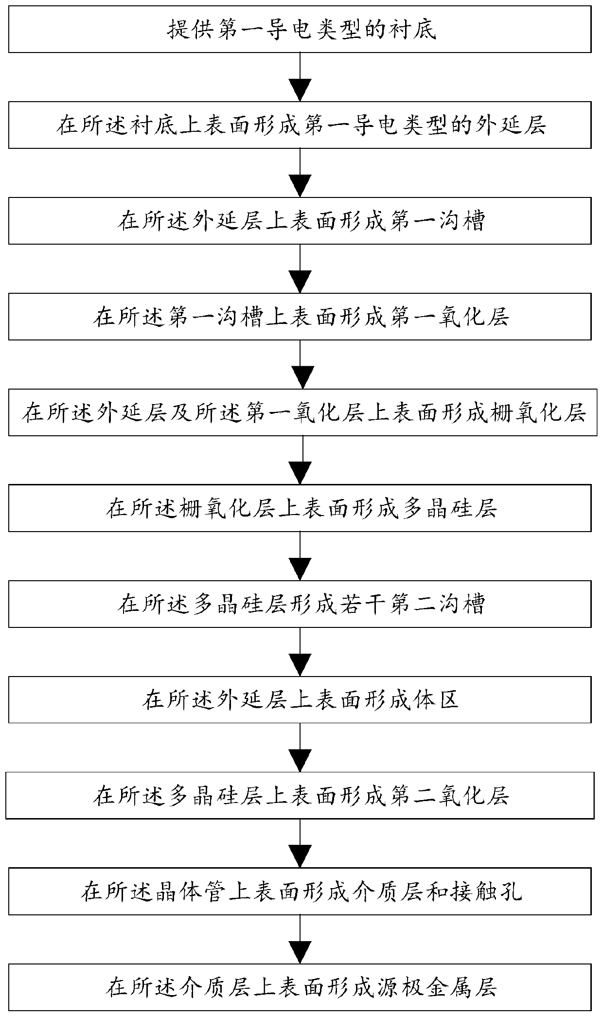
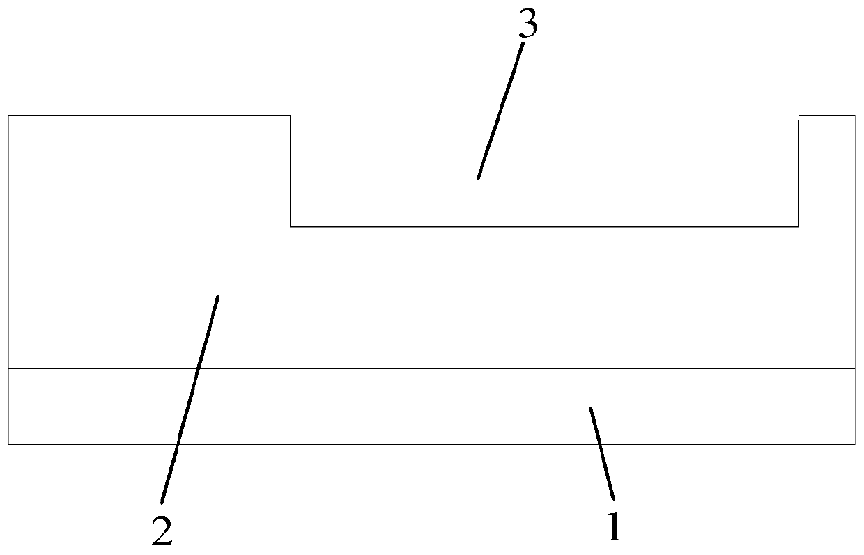
[0026] In order to make the objectives, technical solutions and beneficial technical effects of the present invention clearer, the technical solutions in the embodiments of the present invention will be clearly and completely described below in conjunction with the accompanying drawings in the embodiments of the present invention. Obviously, the described implementation Examples are only some embodiments of the present invention, not all embodiments. Based on the embodiments of the present invention, all other embodiments obtained by persons of ordinary skill in the art without making creative efforts belong to the protection scope of the present invention.

[0027] In the description of the present invention, it should be noted that the terms "center", "upper", "lower", "left", "right", "vertical", "horizontal", "inner", "outer" etc. The indicated orientation or positional relationship is based on the orientation or positional relationship shown in the drawings, or the orient...


PUM


Abstract

The invention provides a transistor and a manufacturing method of a terminal structure thereof. The method includes the following steps: providing a substrate of a first conductivity type, forming anepitaxial layer of the first conductivity type on the upper surface of the substrate, forming a first trench on the upper surface of the epitaxial layer, forming a first oxide layer on the upper surface of the first trench, forming a gate oxide layer on the upper surfaces of the epitaxial layer and the first oxide layer, forming a polysilicon layer on the upper surface of the gate oxide layer, forming a plurality of second trenches on the polysilicon layer, forming a body region on the upper surface of the epitaxial layer, forming a second oxide layer on the upper surface of the polysilicon layer, forming a dielectric layer and a contact hole on the upper surface of the transistor, and forming a source metal layer on the upper surface of the dielectric layer. According to the scheme of theinvention, the source metal layer is connected with a low potential, the substrate is connected with a positive potential, and once the reverse bias potential difference is larger, a better inversionlayer is formed on the outer side of the polysilicon layer to counteract a strong electric field extending from the body region, and thus the withstand voltage performance of the device is realized.

Description

technical field [0001] The invention relates to the technical field of semiconductors, in particular to a manufacturing method of a semiconductor transistor and a terminal structure thereof. Background technique [0002] The withstand voltage capability of a power device mainly depends on the reverse bias breakdown voltage of a specific PN junction in the device structure, and in order to obtain a certain current capability, a power device is usually composed of many cells connected in parallel. When the device reverses the withstand voltage, because the transverse electric field between the cells cancels each other, because the breakdown generally does not occur inside the cell, but the outermost cell will break down due to the concentration of the electric field, so A specific structure is required to reduce the electric field and thus increase the breakdown voltage. These special structures are called terminal technology. [0003] Junction terminals can be roughly divide...

Claims


Application Information

Patent Timeline
IPC IPC(8): H01L21/336H01L29/772H01L29/06
Inventor 不公告发明人
Owner 泉州臻美智能科技有限公司
Why Eureka
Try Eureka