Method for preparing display substrate and display substrate

A technology for display substrates and substrates, which is applied in nonlinear optics, instruments, optics, etc., can solve the problem that the preparation method of reflective display substrates cannot be prepared into shapes.

Pending Publication Date: 2019-05-21
BOE TECH GRP CO LTD
View PDF9 Cites 0 Cited by
  • Summary
  • Abstract
  • Description
  • Claims
  • Application Information

AI Technical Summary

Problems solved by technology

[0004] The invention provides a method for preparing a display substrate to solve the problem that

Method used


Image

  • Method for preparing display substrate and display substrate
  • Method for preparing display substrate and display substrate
  • Method for preparing display substrate and display substrate

Examples


Embodiment 1

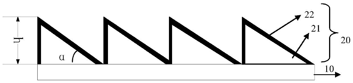
[0033] refer to figure 1 In one aspect, the present invention provides a display substrate, including: a substrate 10 and a reflective layer 20; wherein the reflective layer 20 is disposed on the substrate 10; and the reflective layer includes a plurality of wedge-shaped structures.

[0034] In an embodiment of the present invention, the substrate includes an array substrate.

[0035] In the embodiment of the present invention, the inclined surface of the wedge-shaped structure is a plane or a curved surface, and forms a preset angle α with the substrate.

[0036] In the embodiment of the present invention, the preset included angle α includes: 7°-12°. Preferably, the preset angle α is 9°.

[0037] In an embodiment of the present invention, the height h of the wedge-shaped structure includes: 1 μm-3 μm.

[0038] In the embodiment of the present invention, the reflective layer 20 includes: a resin layer 21 and a reflective layer 22 ; the resin layer 21 is disposed between th...

Embodiment 2

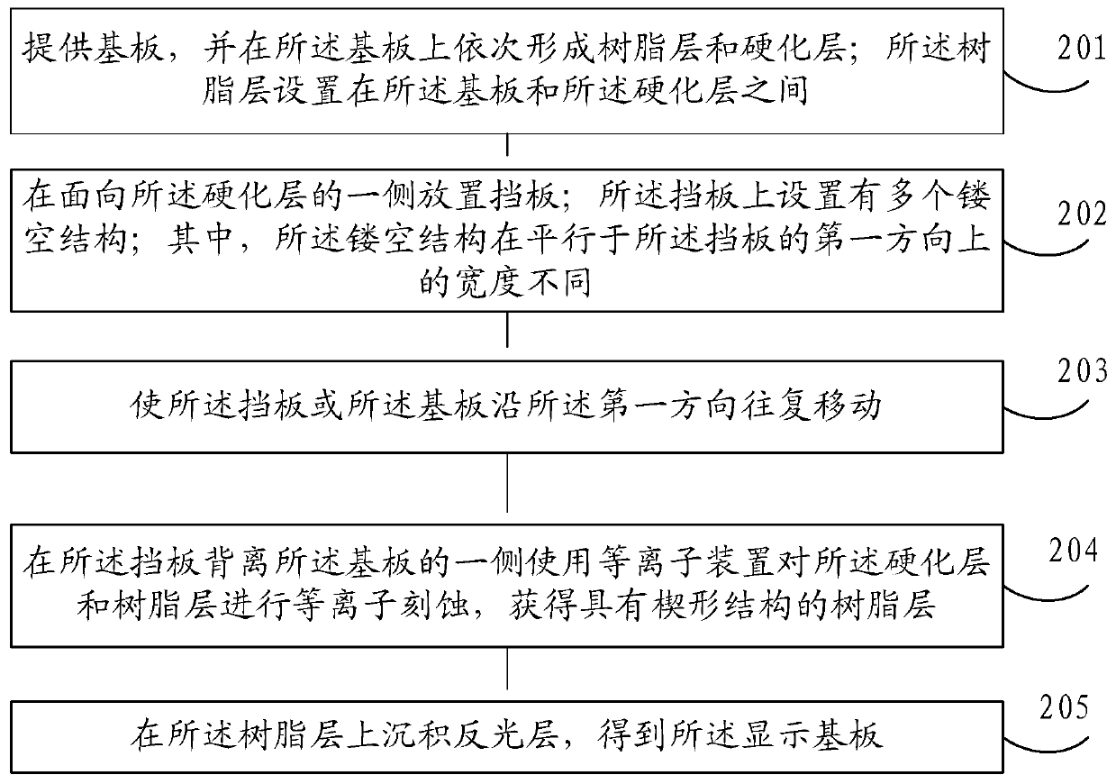
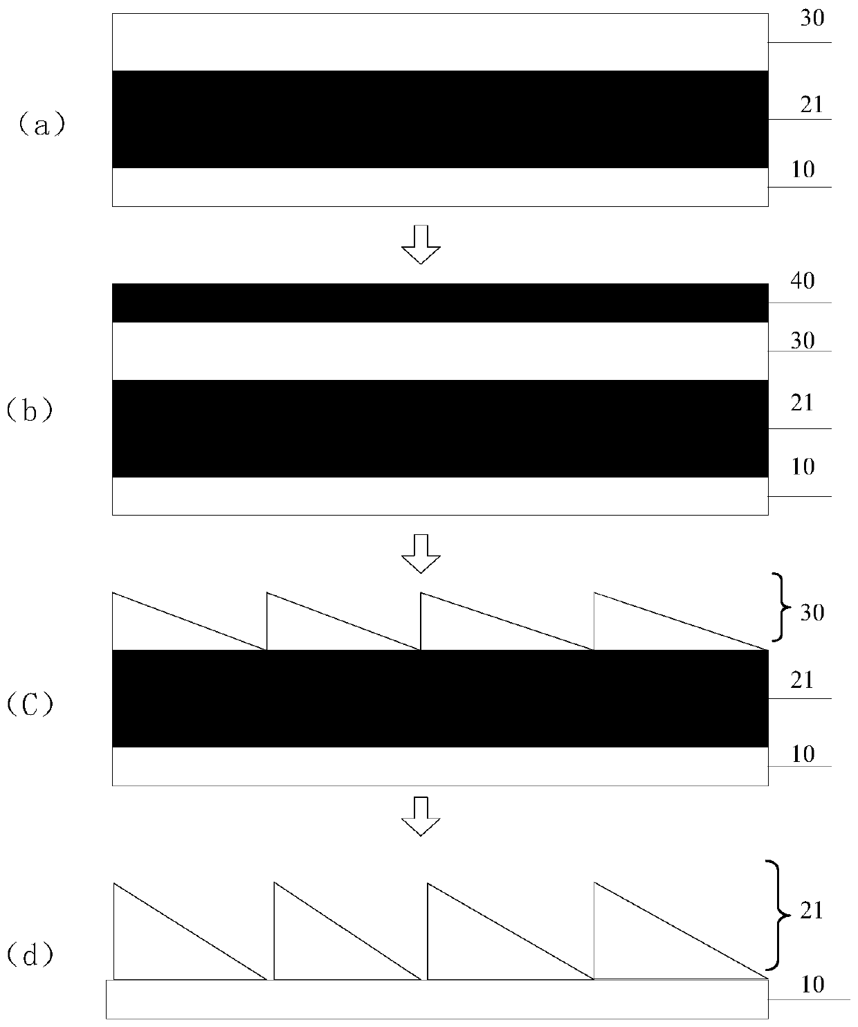
[0042] refer to figure 2 and image 3 An embodiment of the present invention provides a method for preparing a display substrate, including:

[0043] Step 201 , providing a substrate 10 , and sequentially forming a resin layer 21 and a hardened layer 30 on the substrate 10 ; the resin layer 21 is disposed between the substrate 10 and the hardened layer 30 .

[0044] In the embodiment of the present invention, refer to image 3 In (a), the resin layer 21 is coated on the substrate 10, and a hardened layer is deposited on the resin layer 21. The material of the hardened layer 30 includes: silicon dioxide or silicon nitride, preferably silicon dioxide.

[0045] Step 202, placing a baffle 40 on the side facing the hardened layer 30; the baffle 40 is provided with a plurality of hollow structures 41; wherein, the hollow structures 41 are parallel to the first side of the baffle 40 The width in the direction is different.

[0046] In the embodiment of the present invention, ref...


PUM

PropertyMeasurementUnit
Heightaaaaaaaaaa

Abstract

The embodiment of the invention provides a method for preparing a display substrate and a display substrate. The preparation method comprises: providing a substrate and sequentially forming a resin layer arranged between the substrate and a hardened layer and a hardened layer on the substrate; arranging a baffle at one side, facing the hardened layer; arranging a plurality of hollow structures having different width in a first direction parallel to the baffle at the baffle; moving the baffle or the substrate bank and forth in the first direction; carrying out plasma etching on the hardened layer and the resin layer at one side, away from the substrate, of the substrate by using a plasma device to obtain a resin layer having a wedge-shaped structure; and depositing a light-reflecting layeron the resin layer to obtain a display substrate. Therefore, the reflective surface of the resin layer becomes smooth; the effective reflection surface is increased; and thus the utilization ratio oflight is improved.

Description

technical field [0001] The invention relates to the field of display technology, in particular to a method for preparing a display substrate and the display substrate. Background technique [0002] Reflective liquid crystal display (R-LCD) is an LCD panel that uses external light reflection for display. Compared with a transmissive LCD device with a backlight, R-LCD has no backlight, reduces power consumption, and uses natural reflection display. Good for vision protection. The structure of R-LCD mainly includes: color filter substrate, liquid crystal layer, array substrate and reflective layer. [0003] At present, the reflective layer is only prepared by drying on the array substrate, but the resin material has fluidity during the drying process in this way, and it is difficult to obtain the desired shape. Contents of the invention [0004] The invention provides a method for preparing a display substrate to solve the problem that the existing method for preparing a re...

Claims


Application Information

Patent Timeline
IPC IPC(8): G02F1/1335G02F1/1333
Inventor 董立文宋吉鹏张锋孟德天
Owner BOE TECH GRP CO LTD
Why Eureka
Try Eureka