Method for forming bonding structure between wafers and wafer bonding method

A bonding structure and wafer technology, applied in the formation of inter-wafer bonding structure, wafer bonding field, can solve the problems such as difficult to guarantee the bonding strength, achieve high bonding strength, improve the effect of strength

Active Publication Date: 2019-04-26
YANGTZE MEMORY TECH CO LTD
View PDF2 Cites 2 Cited by
  • Summary
  • Abstract
  • Description
  • Claims
  • Application Information

AI Technical Summary

Problems solved by technology

[0004] However, when the existing metal-metal bonding method is used to form a three-dimensional packaging structure, the surface of the bonding metal layer is prone to dishing defects. When the first wafer and the second wafer are bonded, It is difficult to guarantee the strength of the bond

Method used


Image

  • Method for forming bonding structure between wafers and wafer bonding method
  • Method for forming bonding structure between wafers and wafer bonding method
  • Method for forming bonding structure between wafers and wafer bonding method

Examples


Embodiment Construction

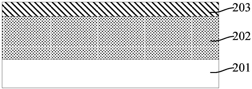
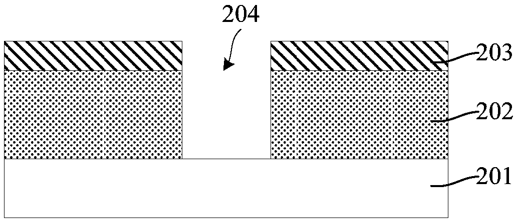
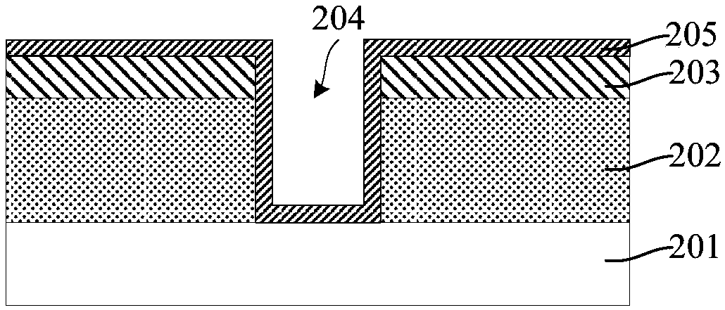
[0028] As mentioned in the background art, copper dishing defects are likely to occur on the surface of the bonding metal layer, and it is difficult to guarantee the bonding strength when wafers are bonded.

[0029] Research has found that when forming an insulating layer and a bonding metal layer in the insulating layer, the material of the insulating layer is usually silicon nitride, and the material of the metal layer is copper. The process of forming the bonding metal layer includes: A through hole (or groove) is formed in the layer; an electroplating process is used to form a metal layer covering the insulating layer, and the metal layer fills the through hole (or groove); a chemical mechanical polishing process is used to planarize the metal layer to The surface of the insulating layer acts as a stop layer, forming a bonding metal layer in the via hole (or trench). During the chemical mechanical polishing process, due to the low grinding rate of the insulating layer of t...


PUM


Abstract

The invention provides a method for forming a bonding structure between wafers and a wafer bonding method. The method for forming the bonding structure between the wafers comprises the steps that a substrate is provided; a stopping layer is formed on the substrate, wherein a through hole is formed in the stopping layer, and the grinding ratio of the stopping layer to a metal material layer is higher than the grinding ratio of silicon nitride to the meta material layer; the metal material layer is formed on the stopping layer, wherein the through hole is filled with the metal material layer; planarization is conducted from the metal material layer to the stopping layer, a bonding metal layer is formed in the through hole, and the bonding structure is formed by the bonding metal layer and the stopping layer on the two sides of the bonding metal layer. By means of the method, dishing defects on the surface of the bonding metal layer are prevented, and the bonding strength is improved.

Description

technical field [0001] The invention relates to the field of semiconductor manufacturing, in particular to a method for forming a bonding structure between wafers and a method for bonding wafers. Background technique [0002] With the requirements of high integration and multi-functionality of microelectronic devices, the existing two-dimensional packaging technology is difficult to meet the packaging requirements, while three-dimensional packaging has the advantages of small size, light weight, and reduced signal delay, and is becoming a microelectronic device packaging technology. mainstream technology. Bonding is the key process to achieve three-dimensional packaging. There are many bonding methods used in three-dimensional packaging, including: metal-metal bonding, oxide direct bonding, anodic bonding, adhesive bonding, and solder-based bonding , ultrasonic bonding, glass dielectric bonding, etc. Metal-metal bonding is widely used in three-dimensional packaging structu...

Claims


Application Information

Patent Timeline
Patent Type & Authority Applications(China)
IPC IPC(8): H01L21/18
CPCH01L21/185H01L21/76831H01L23/528H01L23/5329H01L21/762H01L2221/1057
Inventor 高林蒋阳波王光毅
Owner YANGTZE MEMORY TECH CO LTD
Why Eureka
Try Eureka