Method and device for processing reticle in computational lithography

A computational lithography and reticle technology, which is applied in the field of computational lithography and can solve problems such as low efficiency of computational lithography

Active Publication Date: 2020-12-04
MOYAN COMPUTATIONAL SCI NANJING PTE LTD
View PDF6 Cites 0 Cited by
  • Summary
  • Abstract
  • Description
  • Claims
  • Application Information

AI Technical Summary

Problems solved by technology

[0006] In order to solve the problem that the processing method of the reticle in the prior art requires a lot of time and space to store, read and transmit the basic graphics, and makes the efficiency of computational lithography low, the application discloses a computational lithography Mask processing method and device

Method used


Image

  • Method and device for processing reticle in computational lithography
  • Method and device for processing reticle in computational lithography
  • Method and device for processing reticle in computational lithography

Examples


Embodiment Construction

[0093] In order to solve the problem that the processing method of the reticle in the prior art requires a lot of time and space to store, read and transmit the basic graphics, and makes the efficiency of computational lithography low, the application discloses a computational lithography Mask processing method and device.

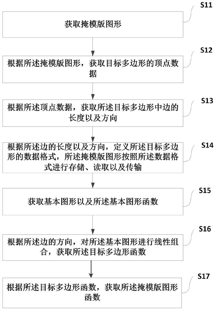
[0094] see figure 1 As shown in the schematic diagram of the workflow, the first embodiment of the present application discloses a method for processing a reticle in computational lithography, including:

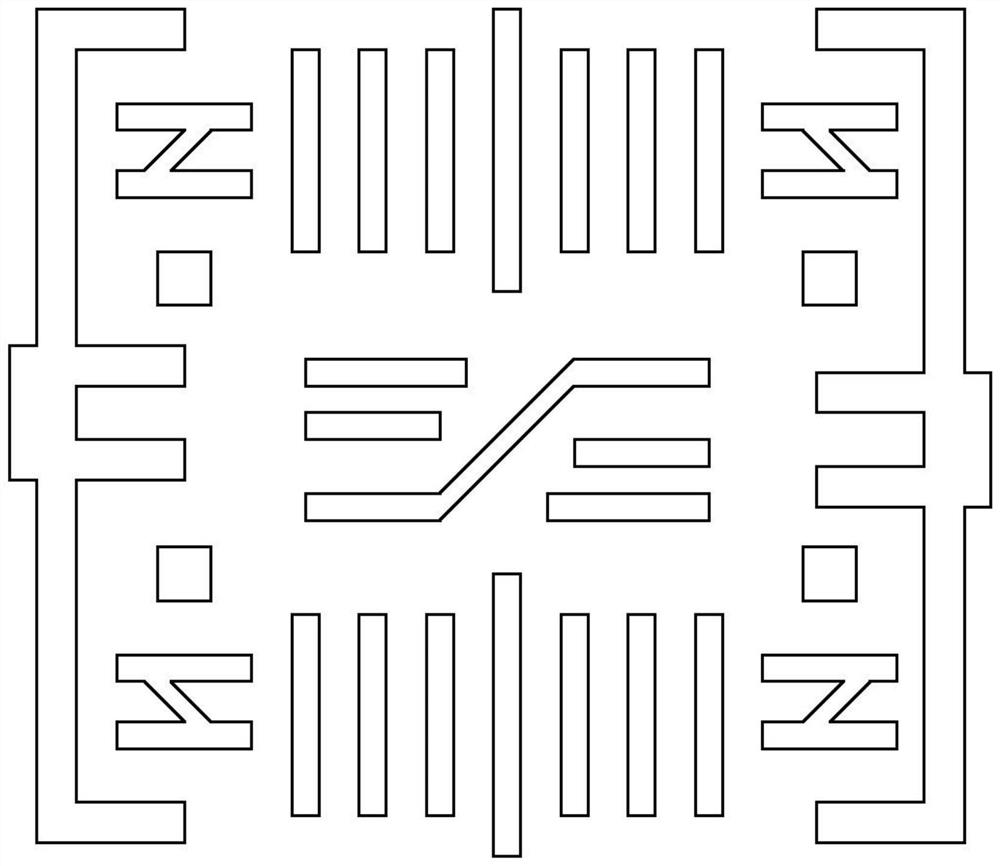
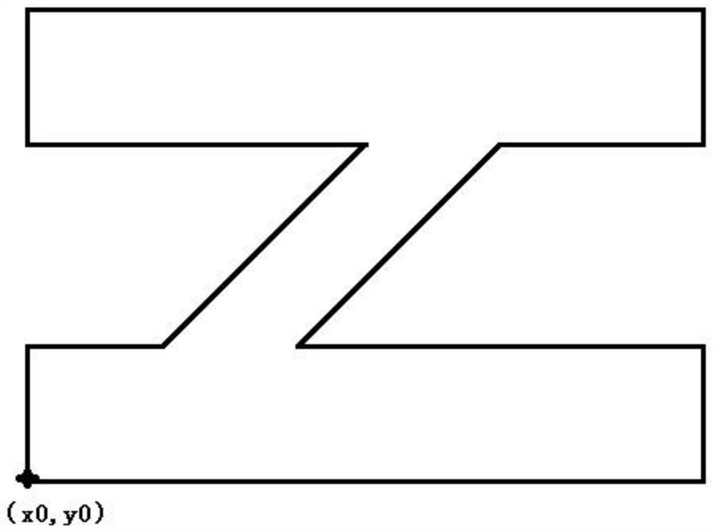
[0095] Step S11, acquiring a reticle pattern, wherein the reticle pattern includes a plurality of polygons.

[0096] The mask (Mask) is an indispensable part in the photolithography process. Pre-designed patterns are processed on the mask, and light passes through it to transmit the pre-designed patterns on the surface of the wafer. The original unprocessed mask is a transparent glass / quartz substrate, and the pre-designed graphics are drawn by corresp...


PUM


Abstract

The present application discloses a mask plate processing method and device in computational lithography. The method comprises acquiring the length and the direction of the side of a polygon by the vertex data of the polygon; defining the data format of the polygon according to the length and the direction of the side; and enabling a mask plate pattern to perform storage, reading, and transmissionin accordance with the data format. Compared with the prior art, the method disclosed in the present application reduces the storage space of the mask plate pattern by storing the sides of the polygon in the mask plate pattern, and enables the fast reading and transfer of the data of the mask plate pattern between computer programs. Moreover, when a mask plate pattern function is obtained, a basic pattern function is linearly combined based on the direction of the sides in the polygon, thereby improving the efficiency of the computational lithography.

Description

technical field [0001] The present application relates to the technical field of computational lithography, and in particular to a method and device for processing a reticle in computational lithography. Background technique [0002] The lithography process is an important process step in the manufacture of integrated circuits. By using the principle of photochemical reaction, the pre-designed pattern on the mask plate is transferred to the surface of the wafer. The main process can be reflected by the lithography model. The lithography model Including: light source, condenser lens, reticle, projection pupil, projection lens and wafer. Combined with the lithography model, the lithography process includes: the light emitted from each light source passes through the condenser lens and becomes parallel light, and the parallel light is irradiated on the mask plate, so that the pattern on the mask plate passes through the projection pupil and the projection lens , is imaged on t...

Claims


Application Information

Patent Timeline
Patent Type & Authority Patents(China)
IPC IPC(8): G03F7/20
CPCG03F7/705G03F7/70508
Inventor 阎江梁文青
Owner MOYAN COMPUTATIONAL SCI NANJING PTE LTD
Why Eureka
Try Eureka