Inverse LED chip and fabrication method thereof

A LED chip and flip-chip technology, which is applied in the direction of electrical components, circuits, semiconductor devices, etc., can solve the problems of N-type pad conduction, etc., and achieve the effect of improving reliability and reducing the probability of conduction

Active Publication Date: 2019-04-12
HC SEMITEK SUZHOU
View PDF4 Cites 1 Cited by
  • Summary
  • Abstract
  • Description
  • Claims
  • Application Information

AI Technical Summary

Problems solved by technology

[0007] Embodiments of the present invention provide a flip-chip LED chip and a manufacturing method thereof, which can solve the problem of conduction between N-type pads and P-type pads in the prior art

Method used


Image

  • Inverse LED chip and fabrication method thereof
  • Inverse LED chip and fabrication method thereof
  • Inverse LED chip and fabrication method thereof

Examples


Embodiment Construction

[0038] In order to make the object, technical solution and advantages of the present invention clearer, the implementation manner of the present invention will be further described in detail below in conjunction with the accompanying drawings.

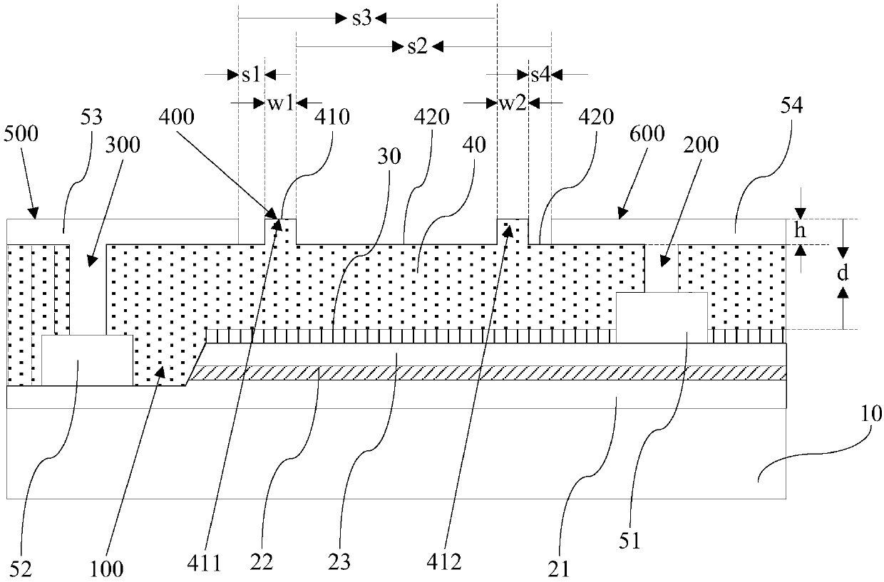
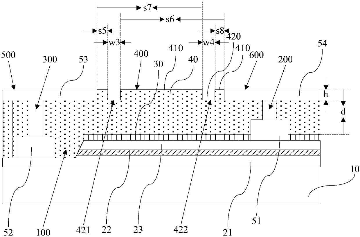
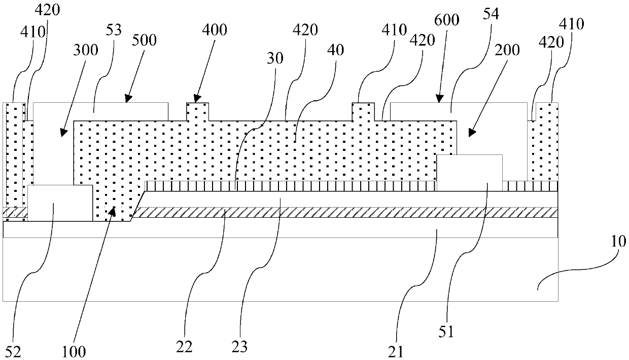
[0039] An embodiment of the present invention provides a flip-chip LED chip. figure 1 It is a schematic structural diagram of a flip-chip LED chip provided by an embodiment of the present invention. see figure 1, the flip-chip LED chip includes a substrate 10, an N-type semiconductor layer 21, an active layer 22, a P-type semiconductor layer 23, a reflective layer 30, an insulating layer 40, a P-type electrode 51, an N-type electrode 52, and an N-type pad 53 and P-type pad 54. The N-type semiconductor layer 21 , the active layer 22 and the P-type semiconductor layer 23 are sequentially stacked on the substrate 10 , and the P-type semiconductor layer 23 is provided with a groove 100 extending to the N-type semiconductor layer 21 . Th...


PUM


Abstract

The invention discloses an inverse LED chip and a fabrication method thereof, and belongs to the technical field of semiconductors. The inverse LED chip comprises a substrate, an N-type semiconductorlayer, an active layer, a P-type semiconductor layer, a reflection layer, an insulation layer, a P-type electrode, an N-type electrode, an N-type bonding pad and a P-type bonding pad, wherein an uppersurface of the insulation layer, an upper surface of the N-type bonding pad and an upper surface of the P-type bonding pad are arranged at the same plane. By arranging the upper surface of the insulation layer, the upper surface of the N-type bonding pad and the upper surface of the N-type bonding pad at the same plane, the state that lead paste is directly extruded between the two bonding pads during pasting the bonding pads and a support can be improved, the probability of conduction of the N-type bonding pad and the N-type bonding pad is reduced, and the reliability of the inverse chip isimproved.

Description

technical field [0001] The invention relates to the technical field of semiconductors, in particular to a flip-chip LED chip and a manufacturing method thereof. Background technique [0002] Light Emitting Diode (English: Light Emitting Diode, referred to as: LED) is a semiconductor diode that can convert electrical energy into light energy. As a new type of light-emitting device, LED technology has developed rapidly, has a wide range of application fields, has strong industrial driving force, and has great energy-saving potential. It meets the requirements of low-carbon ecological economy and the development trend of contemporary emerging industries. Compared with traditional electric lighting, LED lighting has the advantages of energy saving, environmental protection, longevity and high efficiency, and is recognized by various countries as the most promising lighting industry. [0003] The chip is the core component of the LED, which is divided into three types: front-mou...

Claims


Application Information

Patent Timeline
Patent Type & Authority Applications(China)
IPC IPC(8): H01L33/44H01L33/38
CPCH01L33/38H01L33/44H01L2933/0016H01L2933/0025
Inventor 张威王江波
Owner HC SEMITEK SUZHOU
Why Eureka
Try Eureka