
Patsnap Eureka
For R&D, Patsnap Eureka makes reading and utilizing patents & technical documents easy.
Patsnap Eureka AIR
Designed for self-driven R&D workflows. Generate viable solutions, solve complex R&D challenges, empower your innovation with AI.

Patsnap Eureka Materials
Designed for material experts only. Revolutionize your material R&D, from search, analyze, to developing new materials.

TechResearch
Generate reliable direction feasibility study reports for your R&D in just a few steps.

TechSeek
Discover and master advanced knowledge NOW. Basics, ideas, possibilities, all at once.

TechMind
As an expert in R&D Theories, TechMind can generates customized viable solutions instantly.

TechRisk
Analyze your overall solution with one click, know your potential R&D risks in advance.

TechMonitor
Get weekly tech updates, stay abreast of the latest tech innovations and key insights.
Display panel and manufacturing method thereof
A technology for a display panel and a manufacturing method, which is applied in the photoengraving process, optics, instruments and other directions of the pattern surface, can solve problems such as affecting the orderly arrangement of liquid crystals, poor liquid crystals, and reducing the yield of finished products, and achieves improvement of product quality and product quality. Yield, reducing the angle difference, eliminating the effect of the formation of liquid crystal bubbles
- Summary
- Abstract
- Description
- Claims
- Application Information
AI Technical Summary
Problems solved by technology
Method used
Image

Examples
Embodiment Construction
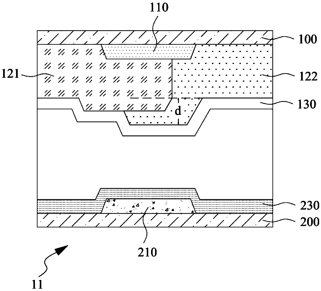
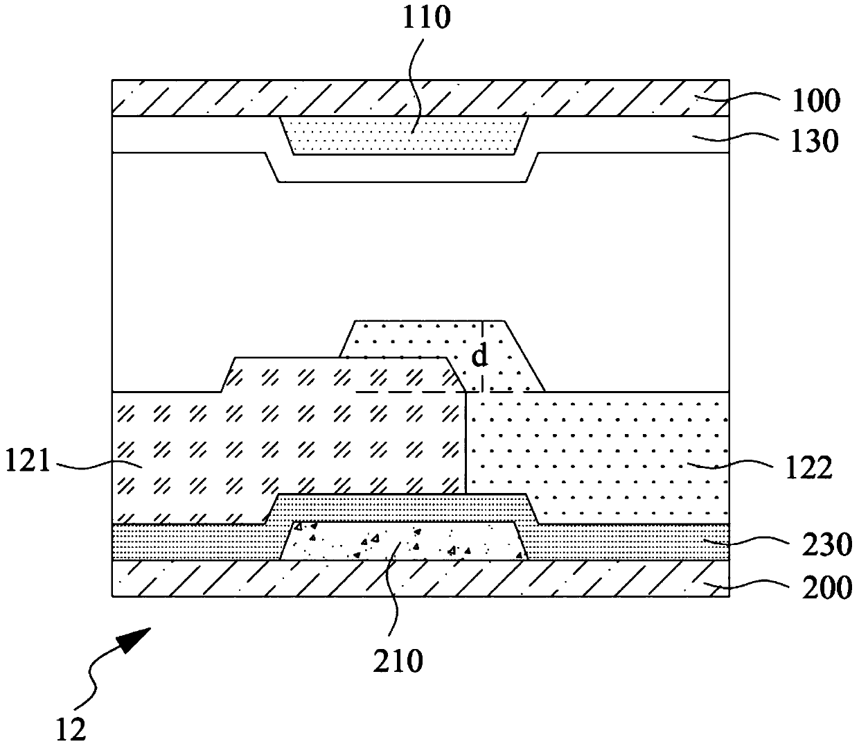
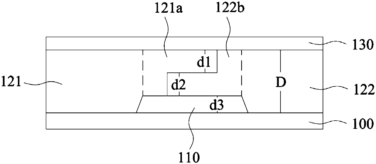
[0027] The following descriptions of the various embodiments refer to the attached drawings to illustrate specific embodiments that the present application can be implemented in. The directional terms mentioned in this application, such as "up", "down", "front", "rear", "left", "right", "inside", "outside", "side", etc., are for reference only The orientation of the attached schema. Therefore, the directional terms used are used to illustrate and understand the application, but not to limit the application.
[0028] The drawings and descriptions are to be regarded as illustrative in nature and not restrictive. In the figures, structurally similar units are denoted by the same reference numerals. In addition, the size and thickness of each component shown in the drawings are arbitrarily shown for understanding and convenience of description, but the present application is not limited thereto.
[0029] In the drawings, the thickness of layers, films, panels, regions, etc., ar...
PUM
 Abstract
Description
Claims
Application Information
 - R&D Engineer
- R&D Manager
- IP Professional
- Industry Leading Data Capabilities
- Powerful AI technology
- Patent DNA Extraction
Browse by: Latest US Patents, China's latest patents, Technical Efficacy Thesaurus, Application Domain, Technology Topic, Popular Technical Reports.
© 2024 PatSnap. All rights reserved.Legal|Privacy policy|Modern Slavery Act Transparency Statement|Sitemap|About US| Contact US: help@patsnap.com