Eureka AIR delivers breakthrough ideas for toughest innovation challenges, trusted by R&D personnel around the world.

A resistive random access memory

A technology of resistive memory and resistive layer, applied in electrical components and other directions, can solve the problems of increasing device storage speed, low setting speed, and reducing resistance state retention characteristics and stability.

Active Publication Date: 2019-04-05
INST OF MICROELECTRONICS CHINESE ACAD OF SCI
View PDF5 Cites 2 Cited by
  • Summary
  • Abstract
  • Description
  • Claims
  • Application Information

AI Technical Summary

Problems solved by technology

[0003] In the prior art, due to many reasons such as the random formation of conductive thin wires of the non-volatile resistive memory, the memory characteristics of the resistive memory are greatly weakened, and then Reduced retention characteristics and stability of the resistance state
In addition, the high set voltage of the resistive memory in the prior art is not conducive to the realization of low power consumption characteristics of the device, and the low set speed is not conducive to the improvement of the storage speed of the device, which seriously restricts the resistive performance of the resistive memory.

Method used


Image

  • A resistive random access memory

Examples


Embodiment Construction

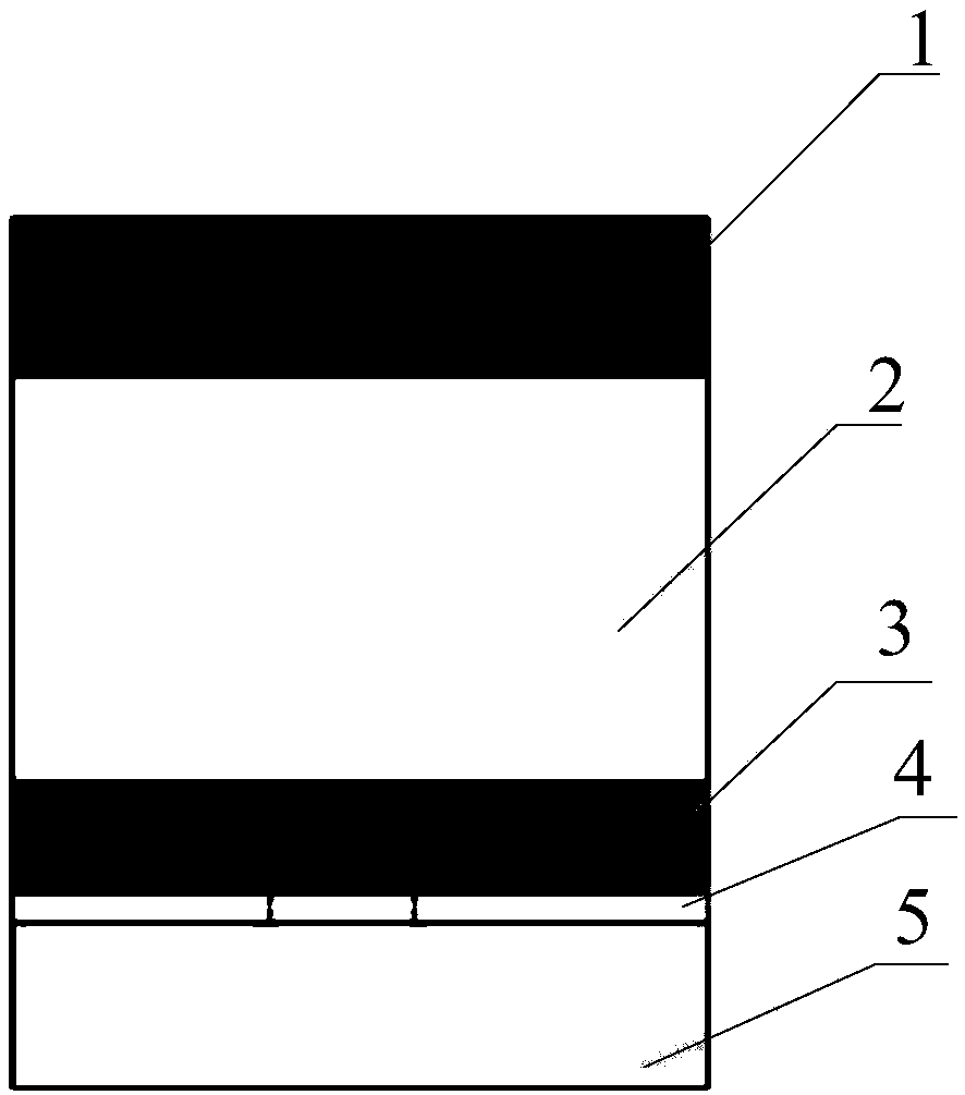
[0022] In order to improve the resistive performance of the resistive variable memory, an embodiment of the present invention provides a resistive variable memory, which includes: a first electrode layer; a resistive variable layer located below the first electrode layer; a first an intermediate layer located below the resistive layer, and the mobility of the first intermediate layer is less than 1 cm 2 / Vs; the second intermediate layer is located below the first intermediate layer, and the material of the second intermediate layer includes a two-dimensional material; the second electrode layer is located below the second intermediate layer.

[0023] The technical solution of the present invention will be further described in detail below with reference to the drawings and specific embodiments.

[0024] In order to fully understand the technical solution of this article, this article first introduces the resistive variable memory. The resistive variable memory switches the re...


PUM


Abstract

The present invention provides a resistive random access memory comprising a first electrode layer; the resistive random layer is arranged below the first electrode layer; a first intermediate layer is arranged below the resistive random layer; the mobility of the first intermediate layer is less than 1 cm<2> / Vs; a second intermediate layer is arranged below the first intermediate layer; the materials of the second intermediate layer comprises two-dimensional materials; a second electrode layer is below the second intermediate layer; since the mobility of the first intermediate layer is lessthan 1 cm<2> / Vs, the diffusion speed of metal ions can be slowed down under the action of the electric field, so that a part of the metal ions remain in the first intermediate layer, and conductive thin wires do not completely break under the electric field, thereby reducing volatility of the resistive random access memory during setting or resetting. In setting, since the metal ions in the second electrode layer are easily accumulated in the conductive thin wires in the first intermediate layer and the second intermediate layer, the settling speed is increased; and in each setting process, the conductive thin wires are preferentially formed in the same place to lower the setting voltage.

Description

technical field [0001] The invention relates to the technical field of microelectronic devices, in particular to a resistive variable memory. Background technique [0002] With the rapid development of electronic technology and devices, people urgently need memories with higher storage speed and storage density, and resistive variable memory is one of the current choices. [0003] In the prior art, due to many reasons such as the random formation of conductive thin wires of the non-volatile RRAM, the memory characteristics of the RRAM are greatly weakened, thereby reducing the retention characteristics and stability of the resistive state. In addition, the high set voltage of the resistive variable memory in the prior art is not conducive to realizing the low power consumption characteristics of the device, and the low set speed is not conducive to the improvement of the storage speed of the device, which seriously restricts the resistive variable performance of the resistiv...

Claims


Application Information

Patent Timeline
Patent Type & Authority Applications(China)
IPC IPC(8): H01L45/00
CPCH10N70/801
Inventor 卢年端马尚李泠耿玓刘琦刘明
Owner INST OF MICROELECTRONICS CHINESE ACAD OF SCI
Why Eureka
Eureka Blog
Learn More