Novel silicon carbide junction barrier Schottky diode and fabrication method thereof
A technology of junction barrier Schottky and manufacturing method, which is applied in the field of semiconductor power devices, can solve the problems of low avalanche tolerance of junction barrier diodes, and achieve the effect of improving avalanche tolerance
- Summary
- Abstract
- Description
- Claims
- Application Information
AI Technical Summary
Problems solved by technology
Method used
Image
Examples
Embodiment 1
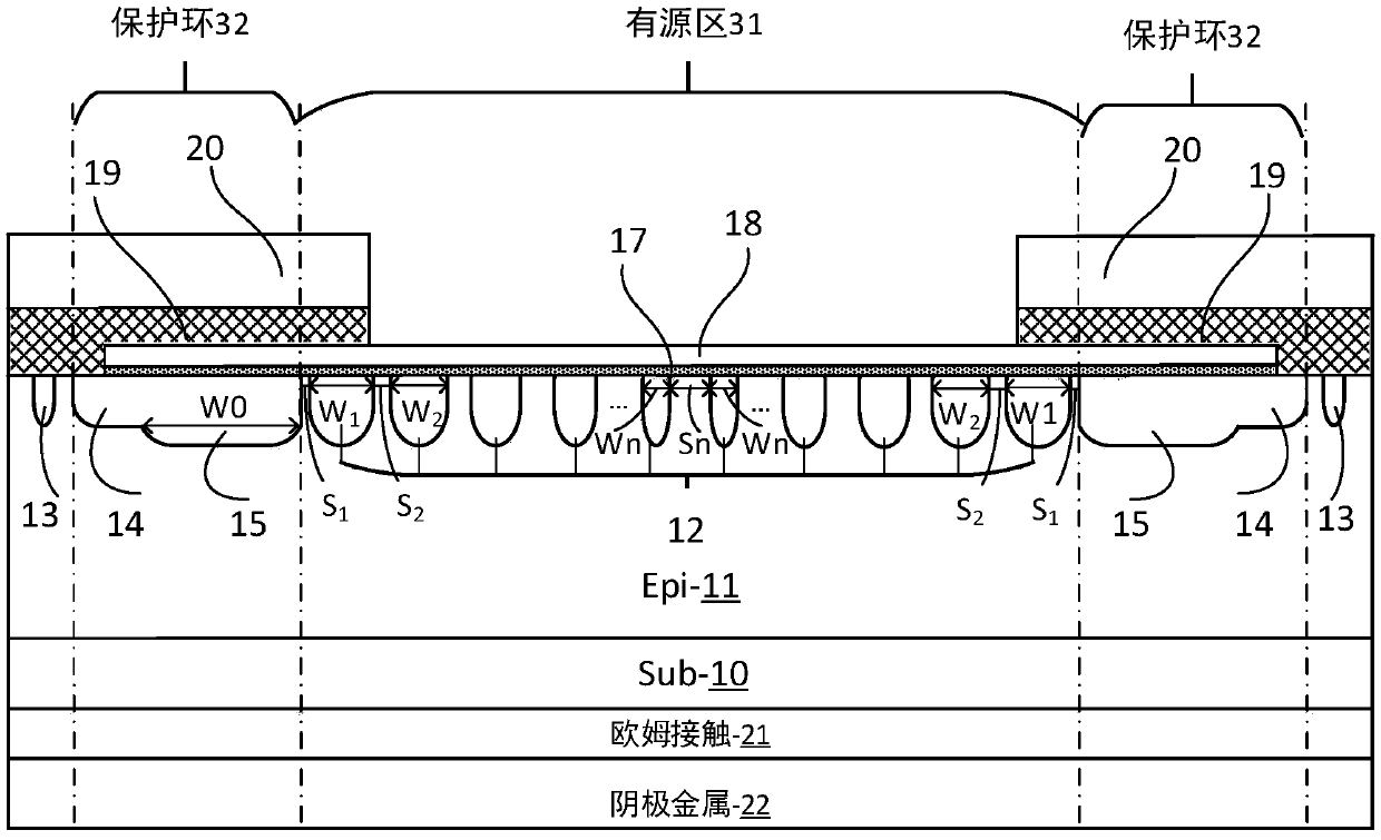
[0038] refer to figure 1 , this embodiment provides a novel silicon carbide junction barrier Schottky diode, comprising a first conductivity type silicon carbide substrate 10 stacked, a first conductivity type silicon carbide epitaxial layer 11; the first conductivity type silicon carbide epitaxial layer The upper surface of the layer 11 is sequentially provided with an active region 31, a guard ring 32 and a second conductivity type terminal field limiting ring 13 from the center to the outside; the active region 31 includes a plurality of second conductivity type junction barriers arranged at intervals District 12;
[0039] Along the direction from the guard ring 32 to the center of the active region 31 , the distance between adjacent junction barrier regions 12 of the second conductivity type gradually increases, and the width of the junction barrier regions 12 of the second conductivity type gradually decreases.
[0040] Specifically, the guard ring 32 is divided into a s...
Embodiment 2
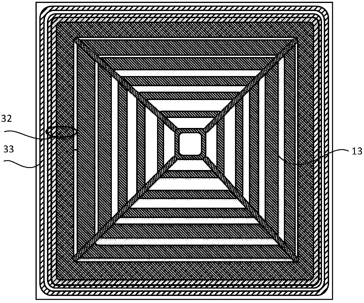
[0045] refer to image 3The difference between this embodiment and Embodiment 1 is that: the junction barrier region 12 of the second conductivity type is ring-shaped, along the direction from the periphery of the guard ring 32 to the center of the active region 31, adjacent to the junction of the second conductivity type The distance between the barrier regions 12 increases gradually, and the width of the junction barrier regions 12 of the second conductivity type gradually decreases.
Embodiment 3
[0047] refer to Figure 4 with 5 , the difference between this embodiment and embodiment 1 is: in this embodiment, each of the second conductivity type junction barrier 12 regions includes two sub-junction barrier regions; the width of the at least two sub-junction barrier regions is the same , the distance between them is also the same; and the distance is equal to the distance between the junction barrier region 12 of the second conductivity type where it is located and the last junction barrier region 12 of the second conductivity type. This forms the structure of group gradients.
PUM
| Property | Measurement | Unit |
|---|---|---|
| electrical resistivity | aaaaa | aaaaa |
Abstract
Description
Claims
Application Information
 - R&D Engineer
- R&D Manager
- IP Professional
- Industry Leading Data Capabilities
- Powerful AI technology
- Patent DNA Extraction
Browse by: Latest US Patents, China's latest patents, Technical Efficacy Thesaurus, Application Domain, Technology Topic, Popular Technical Reports.
© 2024 PatSnap. All rights reserved.Legal|Privacy policy|Modern Slavery Act Transparency Statement|Sitemap|About US| Contact US: help@patsnap.com


