Image sensor and forming method thereof

A technology of image sensor and transmission gate, applied in the direction of electric solid-state devices, semiconductor devices, electrical components, etc., can solve problems such as image lag, and achieve the effect of improving quality

Inactive Publication Date: 2019-04-02
HUAIAN IMAGING DEVICE MFGR CORP
View PDF5 Cites 1 Cited by
  • Summary
  • Abstract
  • Description
  • Claims
  • Application Information

AI Technical Summary

Problems solved by technology

[0005] In the prior art, the full well capacity of the pixel unit is increased by increasing the depth of the PD region. However, the depth of the PD region is limited by the thickness of the second silicon substrate layer in the SOI substrate, and if the depth of the PD region is too deep, it will easily lead to image lag

Method used


Image

  • Image sensor and forming method thereof
  • Image sensor and forming method thereof
  • Image sensor and forming method thereof

Examples


Embodiment Construction

[0025] In the existing image sensor technology, in order to increase the full well capacity of the pixel unit, it is necessary to increase the PD area.

[0026] The inventors of the present invention have found through research that, in the prior art, it is difficult to increase the full well capacity of the pixel unit by directly increasing the depth or width of the PD region.

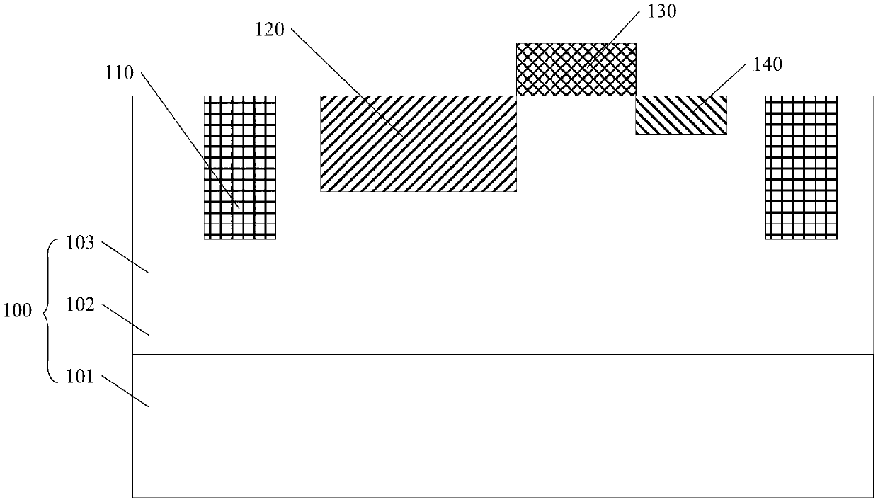
[0027] refer to figure 1 , figure 1 It is a schematic diagram of a device cross-sectional structure of an image sensor in the prior art.

[0028] The image sensor may include a semiconductor substrate 100 , and the semiconductor substrate 100 may include a stacked first silicon substrate layer 101 , a substrate oxide layer 102 and a second silicon substrate layer 103 .

[0029] The image sensor may further include a photodiode doped region 120 , a transfer gate 130 and a floating diffusion region 140 .

[0030] Wherein, the transfer gate can be located on the surface of the second silicon substrate...


PUM


Abstract

The invention provides an image sensor and a forming method thereof. The image sensor comprises: a semiconductor substrate, wherein the semiconductor substrate comprises a first silicon substrate layer, a substrate oxidation layer and a second silicon substrate layer, which are stacked together; a transmission gate located on a surface of the second silicon substrate layer; a floating diffusion region located in the semiconductor substrate on one side of the transmission gate; a photodiode doping region located in the first silicon substrate layer; and a conducting structure located in the semiconductor substrate on the other side of the transmission gate, penetrating through the second silicon substrate layer and the substrate oxidation layer and electrically connected with the photodiode doping region. By adoption of the scheme provided by the invention, higher full well capacity may be obtained.

Description

technical field [0001] The invention relates to the technical field of semiconductor manufacturing, in particular to an image sensor and a forming method thereof. Background technique [0002] In the prior art, in order to better realize dielectric isolation of components in integrated circuits and eliminate parasitic latch-up effects in semiconductor devices, silicon-on-insulator (Silicon on Insulator, SOI) substrates have been widely used. Wherein, the SOI substrate may include a first silicon substrate layer, a substrate oxide layer and a second silicon substrate layer stacked from bottom to top. [0003] In the process of forming a CMOS image sensor (CMOS Image Sensor, CIS) using an SOI substrate, usually only a photodiode (Photo Diode, PD) doped region and a floating diffusion region (Floating Diffusion, FD) are formed in the second silicon substrate layer. ). [0004] However, with the development of smaller pixel units, the full well capacity (Full Well Capacity, FW...

Claims


Application Information

Patent Timeline
Patent Type & Authority Applications(China)
IPC IPC(8): H01L27/146
CPCH01L27/14605H01L27/1461H01L27/14636H01L27/14687H01L27/14692H01L27/14612H01L27/1463H01L27/14689H01L27/14643
Inventor 黄心怡张超
Owner HUAIAN IMAGING DEVICE MFGR CORP
Why Eureka
Try Eureka