Touch panel, manufacturing method thereof and display device

The technology of a touch panel and its manufacturing method is applied in the directions of instruments, electrical digital data processing, electrical components, etc., and can solve the problems that the Y sizes of the touch electrodes are not completely the same, affecting the uniformity of touch control, etc.

Pending Publication Date: 2019-04-02
BOE TECH GRP CO LTD
View PDF0 Cites 2 Cited by
  • Summary
  • Abstract
  • Description
  • Claims
  • Application Information

AI Technical Summary

Problems solved by technology

Moreover, the existence of touch electrode traces makes the size of the touch electrodes Y not exactly the same, which will also affect the touch uniformity.

Method used


Image

  • Touch panel, manufacturing method thereof and display device
  • Touch panel, manufacturing method thereof and display device
  • Touch panel, manufacturing method thereof and display device

Examples


Embodiment Construction

[0048] The specific implementations of the touch panel provided by the embodiments of the present invention, its manufacturing method and the display device will be described in detail below with reference to the accompanying drawings.

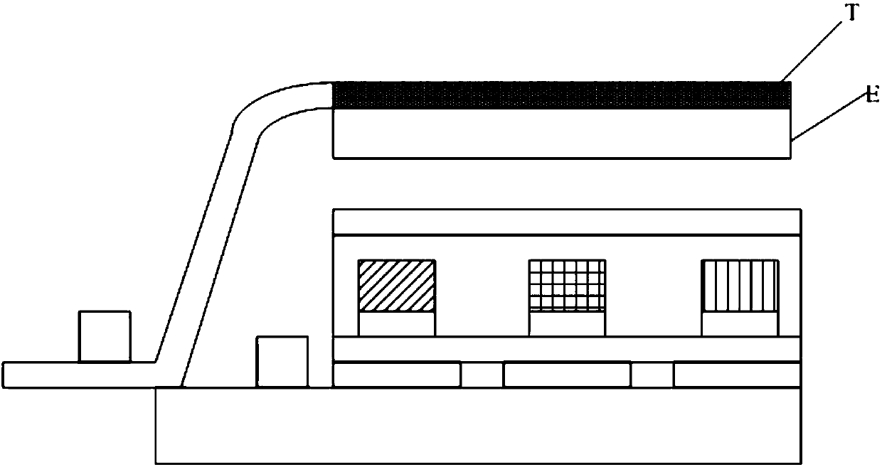
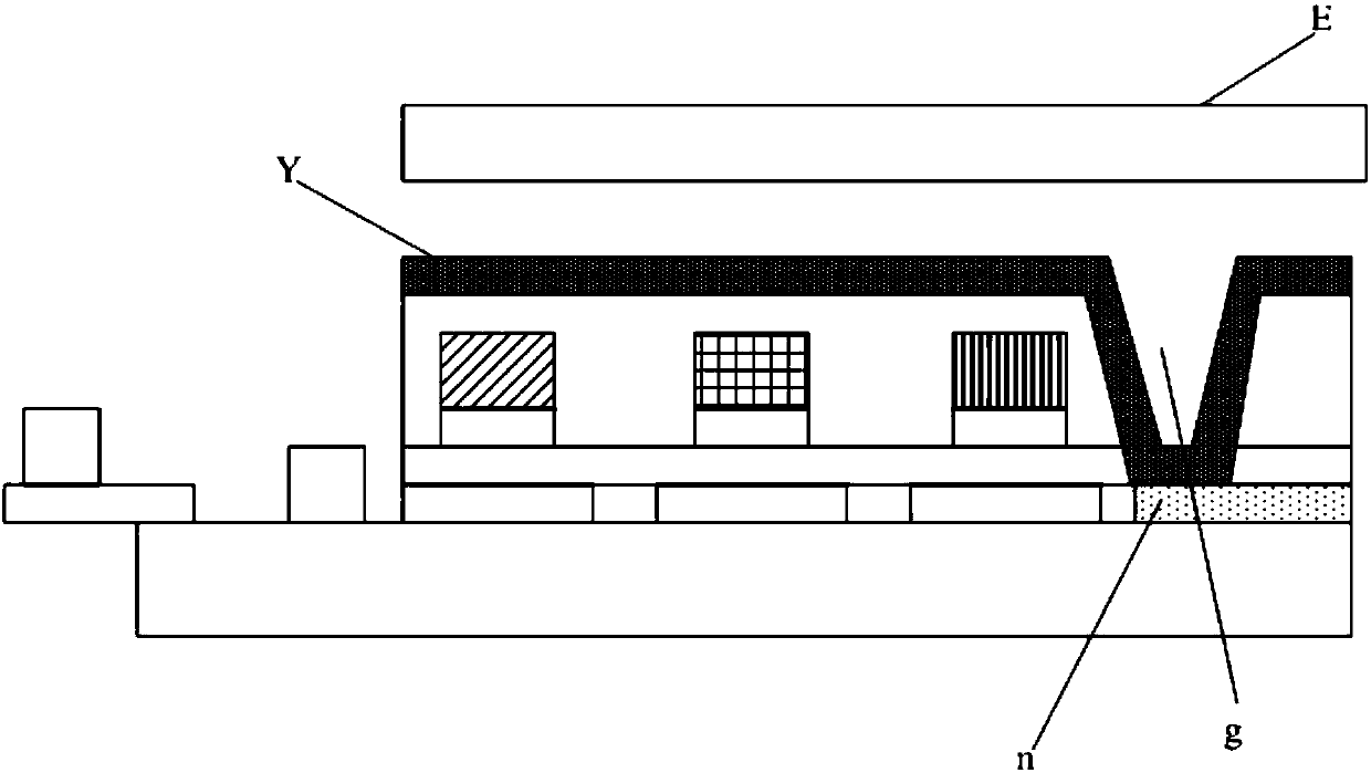
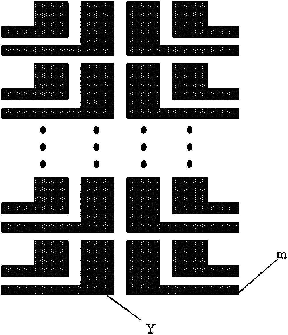
[0049] An embodiment of the present invention provides a touch panel, including: a plurality of spacers located on a base substrate, a plurality of touch electrode traces, a plurality of cathodes arranged in a matrix, and a touch chip; wherein,

[0050] Such as image 3 As shown, the spacer includes: a first support pillar P1 and a second support pillar P2; the first support pillar P1 is located on the substrate substrate, and the second support pillar P2 is located on the first support pillar P1;

[0051] Such as Figure 4 As shown, each cathode Y corresponds to a touch electrode trace; image 3 As shown, each touch electrode trace includes a first lead part L1 and a second lead part L2; the first lead part L1 covers the surface of the firs...


PUM


Abstract

The invention discloses a touch panel, a manufacturing method thereof and a display device. A multiplex cathode of the touch panel is used as a touch electrode, and the cathodes distributed in a matrix mode are connected with a touch chip through touch electrode wires so as to achieve a touch function, wherein the first lead part of the touch electrode wire covers the surface of the first supporting column; so that the cathode can be directly connected with the first lead part; the first lead part can be connected with the touch chip through the second lead part, so that the touch function canbe realized. Compared with the prior art, the touch control electrodes achieve the touch control function through the touch control wires located on the same layer of the peripheries of the touch control electrodes, touch control blind areas can be avoided, meanwhile, a plurality of cathodes which are arranged in a matrix mode and consistent in size are multiplexed as the touch control electrodes, and the problem that due to the fact that the touch control electrodes are not uniform in size, the touch control uniformity is poor is avoided.

Description

technical field [0001] The present invention relates to the field of display technology, in particular to a touch panel, a manufacturing method thereof and a display device. Background technique [0002] With the advancement of display technology, organic light-emitting display (OLED, Organic Light Emitting Diode) is one of the hot spots in the field of flat panel display research today, and more and more active matrix organic light-emitting diodes (AMOLED, Active Matrix Organic Light Emitting Diode) Display panels have entered the market. Compared with traditional thin film transistor liquid crystal display panels (TFT LCD, Thin Film Transistor Liquid Crystal Display), AMOLED has faster response speed, higher contrast ratio and wider viewing angle. [0003] At present, OLEDs have begun to replace traditional LCD displays in display fields such as mobile phones, PDAs, and digital cameras. At the same time, with the progress of the display technology, the in-cell touch techn...

Claims


Application Information

Patent Timeline
IPC IPC(8): G06F3/041
CPCG06F3/0412G06F2203/04103H10K59/8052G06F3/0443G06F3/04164G06F3/0446H10K59/40H10K50/82H10K59/122
Inventor 杨盛际董学陈小川玄明花王磊卢鹏程肖丽刘冬妮于静
Owner BOE TECH GRP CO LTD
Why Eureka
Try Eureka