Eureka AIR delivers breakthrough ideas for toughest innovation challenges, trusted by R&D personnel around the world.

Prepreg lamination design method

A technology of prepreg and design method, applied in the direction of chemical instruments and methods, lamination, layered products, etc., can solve the problems of increased production cost, increased amount of resin glue, increased number of prepregs, etc.

Inactive Publication Date: 2019-03-29
GUANGZHOU FASTPRINT CIRCUIT TECH +1
View PDF6 Cites 3 Cited by
  • Summary
  • Abstract
  • Description
  • Claims
  • Application Information

AI Technical Summary

Problems solved by technology

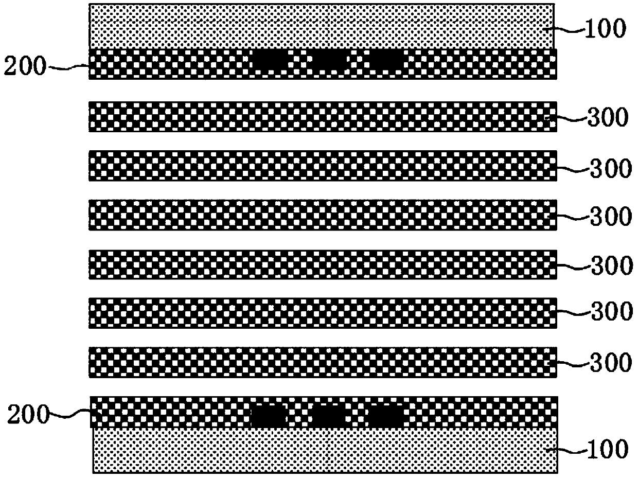
[0003] In actual production, when encountering a thick copper circuit board (copper thickness ≥ 70 μm), especially a rear copper board with a low residual copper rate and a large copper-free area, a larger number of prepregs must be used between layers to meet the requirements. This will lead to two problems: one is that the number of prepregs increases, which means that the amount of resin glue increases, which will lead to increased production costs; the other is that the number of prepregs increases, which can easily lead to lamination. The risk of slippery boards during operation will affect the board quality of the circuit board

Method used


Image

  • Prepreg lamination design method
  • Prepreg lamination design method
  • Prepreg lamination design method

Examples


Embodiment Construction

[0026] In order to make the object, technical solution and advantages of the present invention clearer, the present invention will be further described in detail below in conjunction with the accompanying drawings and specific implementation methods. It should be understood that the specific embodiments described here are only used to explain the present invention, and do not limit the protection scope of the present invention.

[0027] It should be noted that when an element is referred to as being “fixed on”, “disposed on” or “installed on” another element, it may be directly on the other element or there may be an intervening element. When an element is considered to be "connected" to another element, it may be directly connected to the other element or there may be an intervening element at the same time; the specific way that one element is fixedly connected to another element can be realized through existing technologies, and will not be discussed here. To repeat it agai...


PUM

PropertyMeasurementUnit
thicknessaaaaaaaaaa
thicknessaaaaaaaaaa
thicknessaaaaaaaaaa

Abstract

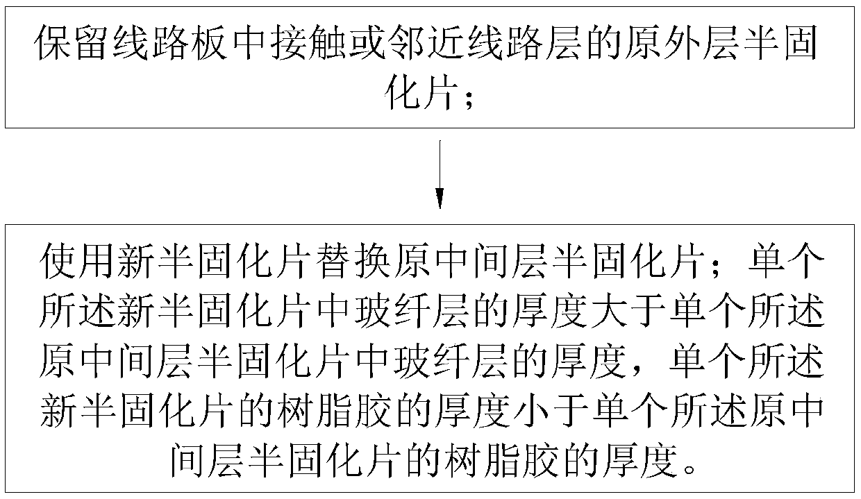
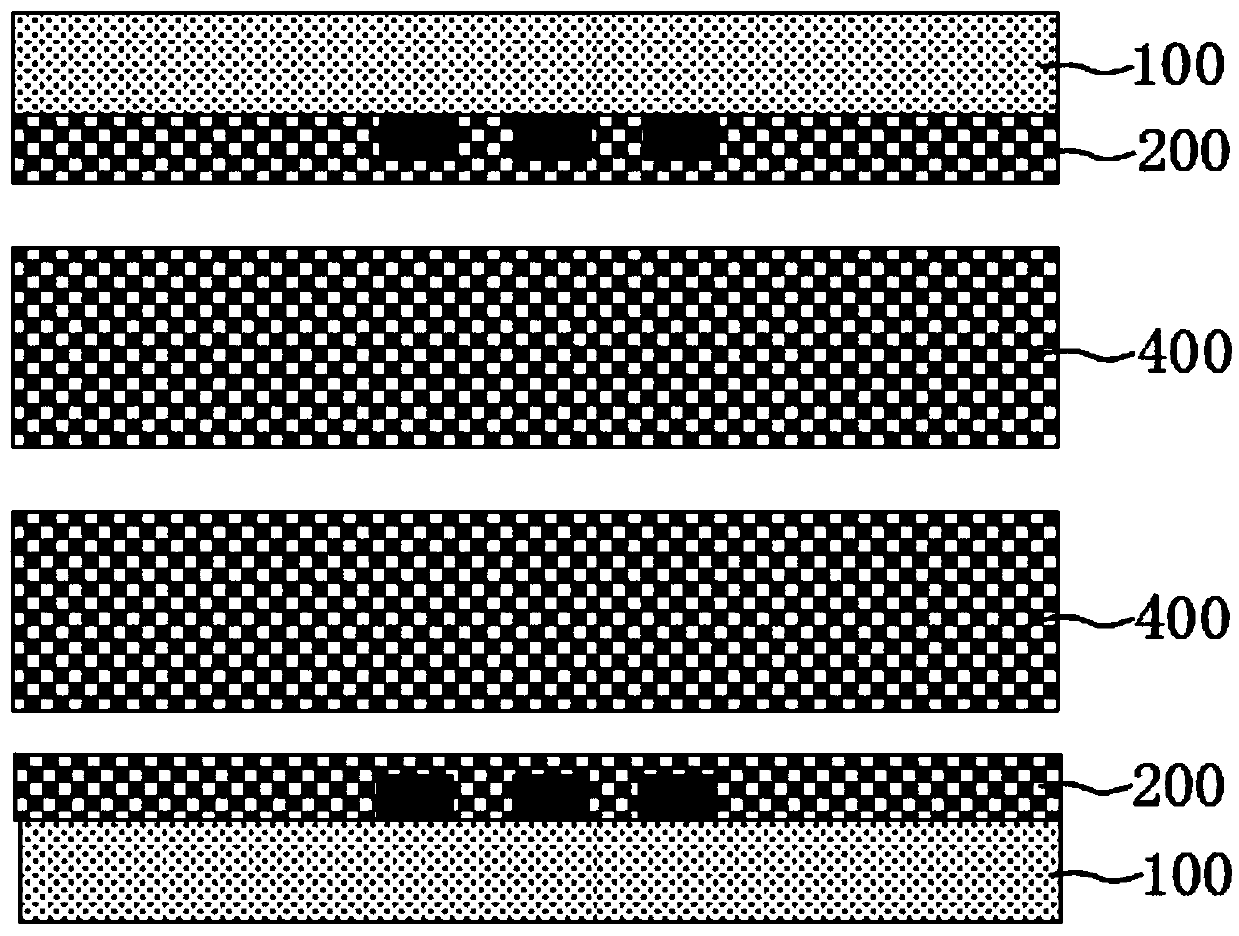
The invention relates to a prepreg lamination design method. The prepreg lamination design method comprises the steps: preserving an original external layer prepreg contacting or adjacent to a circuitlayer in a circuit board; and replacing the original intermediate layer prepreg with a new prepreg, wherein the thickness of a glass fiber layer in the single new prepreg is greater than the thickness of a glass fiber layer in the single original intermediate layer prepreg, and the thickness of the resin glue of the single new prepreg is less than the thickness of the resin paste of the single original intermediate layer prepreg. On the premise of not changing the thickness of the circuit board, the number of new prepregs used can be much less than the number of the original intermediate layer prepregs, thus effectively reducing or eliminating the risk of board sliding caused by excessive lamination during lamination operation, and guaranteeing the quality of the finished circuit board. Moreover, increase of the thickness of the glass fiber layer in the new prepreg effectively compensates for decrease of the thickness of the resin glue caused by the decrease of the number of the original intermediate layer prepregs, thus greatly reducing the use amount of the resin glue, thereby reducing the production cost of the circuit board and improving the operation economical efficiency ofthe circuit board supplier.

Description

technical field [0001] The invention relates to the technical field of printed circuit boards, in particular to a prepreg laminate design method. Background technique [0002] With the continuous development of electronic and electrical products in the direction of intelligence, printed circuit boards are also moving towards multi-layer structures. Multilayer circuit boards generally use prepregs as the bonding medium between layers. However, the type and quantity of prepregs used will be affected by factors such as performance requirements, dielectric thickness, and residual copper ratio. [0003] In actual production, when encountering a thick copper circuit board (copper thickness ≥ 70 μm), especially a rear copper board with a low residual copper rate and a large copper-free area, a larger number of prepregs must be used between layers to meet the requirements. This will lead to two problems: one is that the number of prepregs increases, which means that the amount of r...

Claims


Application Information

Patent Timeline
Patent Type & Authority Applications(China)
IPC IPC(8): H05K1/03B32B17/02B32B17/06B32B33/00B32B37/00
CPCB32B17/02B32B17/06B32B33/00B32B37/00H05K1/036H05K2201/0145H05K2201/0275
Inventor 李泰巍林楚涛李志东
Owner GUANGZHOU FASTPRINT CIRCUIT TECH
Why Eureka
Eureka Blog
Learn More