Semiconductor package device

A technology for packaging devices and semiconductors, applied in semiconductor devices, electrical solid devices, electrical components, etc., can solve the problems of easy peeling off of glue, easy entry into the chip, poor photosensitive effect of the chip, etc., to improve the photosensitive effect, reduce light refraction, The effect of reducing dust-free requirements

Inactive Publication Date: 2019-03-29
NANTONG FUJITSU MICROELECTRONICS
View PDF4 Cites 1 Cited by
  • Summary
  • Abstract
  • Description
  • Claims
  • Application Information

AI Technical Summary

Problems solved by technology

[0003] The inventors of the present application have discovered during long-term research that, on the one hand, since the thickness of the transparent glass cover plate is generally thick, refraction, reflection and energy loss will occur when the light passes through the transparent glass, which will make the photosensitive effect of the chip worse; On the other hand, the transparent glass cover and the chip are connected by glue. After a long time of use, the glue is easy to fall off, and the external dust is easy to enter the photosensitive area of ​​the chip, which will affect the photosensitive effect of the chip.

Method used


Image

  • Semiconductor package device
  • Semiconductor package device
  • Semiconductor package device

Examples


Embodiment Construction

[0024] The following will clearly and completely describe the technical solutions in the embodiments of the present application with reference to the drawings in the embodiments of the present application. Obviously, the described embodiments are only some of the embodiments of the present application, not all of them. Based on the embodiments in this application, all other embodiments obtained by persons of ordinary skill in the art without making creative efforts belong to the scope of protection of this application.

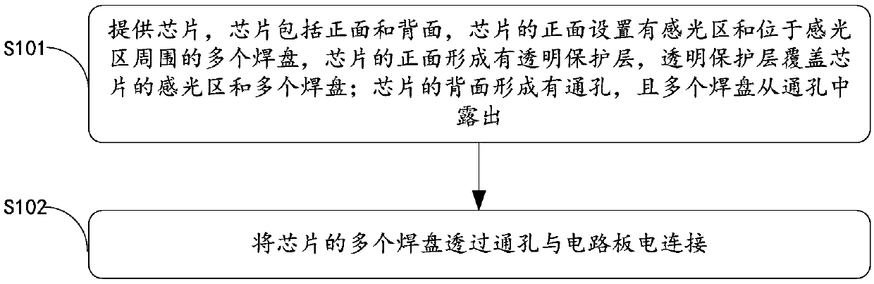
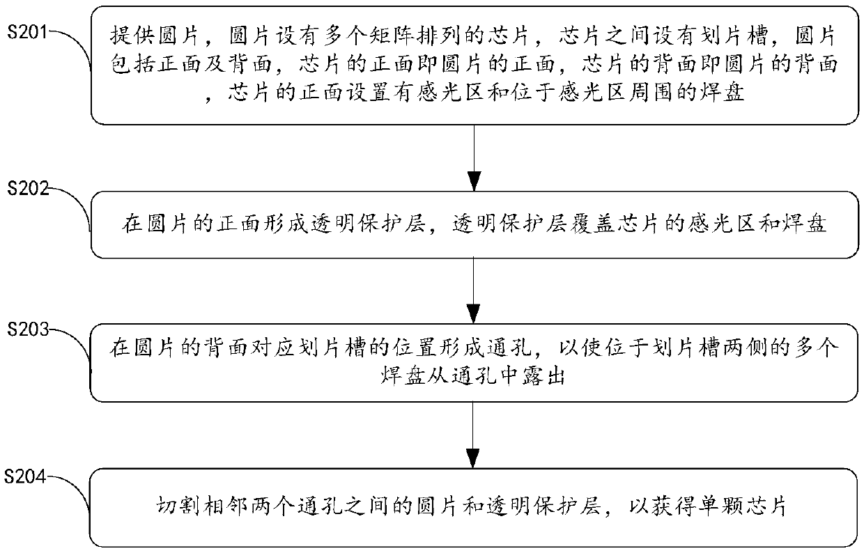
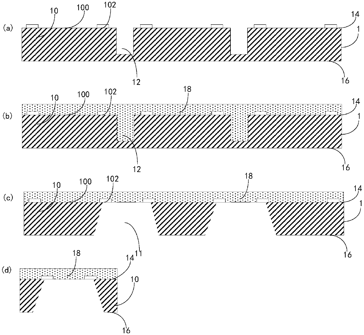
[0025] see figure 1 , figure 1 It is a schematic flow chart of an embodiment of the semiconductor chip packaging method of the present application, the packaging method comprising:

[0026] S101: Provide a chip. The chip includes a front side and a back side. The front side of the chip is provided with a photosensitive area and a plurality of pads located around the photosensitive area. A transparent protective layer is formed on the front side of the chip. ...


PUM


Abstract

The present application discloses a semiconductor package device, and the package device comprises a chip which includes a front surface and a back surface, wherein the front surface of the chip is provided with a photosensitive area and a plurality of bonding pads located around the photosensitive area, the chip is provided with through holes which are corresponding to the positions of the plurality of the bonding pads, and the plurality of the bonding pads of the chip are exposed from the through holes; a transparent protective layer which is located on the front surface of the chip and covers the photosensitive of the chip and the plurality of bonding pads; and a circuit board which is electrically connected to the plurality of the bonding pads of the chip through the through holes. Through the above manner, the device can improve the light sensing effect of the chip.

Description

technical field [0001] The present application relates to the technical field of semiconductors, in particular to a semiconductor packaging device. Background technique [0002] A chip with a photosensitive area is a very important part of an imaging device. In order to protect the photosensitive area of ​​the chip, a commonly used packaging method includes: adding a transparent glass cover above the photosensitive area of ​​the chip to protect the photosensitive area of ​​the chip. [0003] The inventors of the present application have discovered during long-term research that, on the one hand, since the thickness of the transparent glass cover plate is generally thick, refraction, reflection and energy loss will occur when the light passes through the transparent glass, which will make the photosensitive effect of the chip worse; On the other hand, the transparent glass cover and the chip are connected by glue. After a long time of use, the glue is easy to fall off, and ex...

Claims


Application Information

Patent Timeline
IPC IPC(8): H01L27/146
CPCH01L27/14618H01L27/1462
Inventor 俞国庆
Owner NANTONG FUJITSU MICROELECTRONICS
Why Eureka
Try Eureka