A holding method for ultra-thin semiconductor wafers in semiconductor integration process
A semiconductor and ultra-thin technology, applied in the fields of semiconductor devices, semiconductor/solid-state device manufacturing, electric solid-state devices, etc., can solve the problems of fragility, deformation and curling of ultra-thin semiconductor wafers, air bridge structure breakage, etc. The effect of bonding integration yield, reducing the risk of splitting
Active Publication Date: 2021-04-02
南京中电芯谷高频器件产业技术研究院有限公司
View PDF9 Cites 0 Cited by
- Summary
- Abstract
- Description
- Claims
- Application Information
AI Technical Summary
Problems solved by technology
As the thickness of the wafer decreases, the ultra-thin semiconductor wafer itself no longer has enough strength to maintain a flat state. Due to stress and its own gravity, the ultra-thin semiconductor wafer is easily deformed and curled. Fragmentation easily during transfer and processing
In addition, on the surface of semiconductor chips, especially microwave and millimeter wave chips, the wiring of many air bridge structures in the distribution, the stress on the wafer and the resulting large-scale deformation are likely to cause the breakage of the air bridge structure
Method used
View moreImage
Smart ImageViewing Examples

Examples
Embodiment
[0037]A holding method for ultra-thin semiconductor wafers in a semiconductor integrated process, including the following steps:
Login to View More PUM
 Abstract
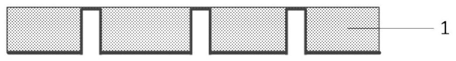
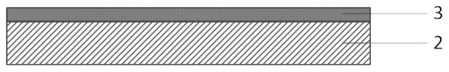
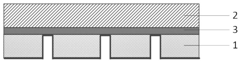
The present application discloses a method for holding an ultra-thin semiconductor wafer (1) in a semiconductor integration process. The main steps comprise: 1) spin-coating a first temporary bonding adhesive (3) on a front surface of a first temporary carrier (2); 2) bonding a front surface of an ultra-thin semiconductor wafer to the front surface of the first temporary carrier; 3) spin-coating a second temporary bonding adhesive (5) on a front surface of a second temporary carrier (4); 4) bonding a rear surface of the ultra-thin semiconductor wafer to the front surface of the second temporary carrier; 5) separating the ultra-thin semiconductor wafer from the first temporary carrier; 6) fabricating an integrated interconnection structure; 7) performing a bonding integration process; and 8) separating the integrated wafer from the second carrier. Two types of temporary bonding adhesives having different softening temperatures are used in conjunction with two temporary carriers, and a temporary bonding process and a bonding release process are used, thereby ensuring that the ultra-thin semiconductor wafer is supported by the temporary carrier during three-dimensional integration processes such as transferring, holding, interconnection structure fabrication, and bonding, and effectively reducing the risk of wafer cracking during the integration process.
Description
Technical field[0001]The present invention belongs to the technical field of semiconductor process, and more particularly to the holding method of the ultra-thin semiconductor wafer in a semiconductor integrated process.Background technique[0002]Semiconductor chip three-dimensional stacking integrated technology is one of the key ways to further miniaturize, light weight, multi-functionalization, and intelligent, and can be reduced by stacking a plurality of semiconductor devices or wafers in a vertical direction. Small system volume, while reducing weight, implementation of overemployment. In general, the wafer to be integrated have been completed or largely completed the technical back and the front, in order to improve the electrical performance of the circuit, improving the heat dissipation efficiency, reduce the package volume and the like, the semiconductor wafer needs to be thinned to 100um or less and even more low. As the thickness of the wafer is lowered, the ultra-thin se...
Claims
Login to View More Application Information
Patent Timeline
 Patent Type & Authority Patents(China)
IPC IPC(8): H01L21/683
CPCH01L21/6835H01L2221/68359H01L2221/68381H01L2221/6835
Inventor 戴家赟吴立枢王飞郭怀新陈堂胜
Owner 南京中电芯谷高频器件产业技术研究院有限公司
Features
- R&D
- Intellectual Property
- Life Sciences
- Materials
- Tech Scout
- Unparalleled Data Quality
- Higher Quality Content
- 60% Fewer Hallucinations
Learn More Browse by: Latest US Patents, China's latest patents, Technical Efficacy Thesaurus, Application Domain, Technology Topic, Popular Technical Reports.
© 2025 PatSnap. All rights reserved.Legal|Privacy policy|Modern Slavery Act Transparency Statement|Sitemap|About US| Contact US: help@patsnap.com