Ultraviolet LED packaging structures
A technology of LED packaging and LED chips, which is applied in the direction of electrical components, electric solid devices, circuits, etc., can solve the problems of rising manufacturing costs, limited heat dissipation, lack of gas flow on the surface of LED chips, etc., so as to improve the service life and improve the overall performance , Eliminate the effect of reducing efficiency and life
- Summary
- Abstract
- Description
- Claims
- Application Information
AI Technical Summary
Problems solved by technology
Method used
Image
Examples
Embodiment 1
[0025] Please combine figure 1 As shown, the ultraviolet LED packaging structure involved in this embodiment includes a substrate 101 and a light-transmitting housing 102. The light-transmitting housing 102 is made of quartz glass, which can be a six-sided closed cuboid structure to form a closed space 107. Buckle, riveting, gluing and other combinations. In addition, the airtight space 107 can be formed by the transparent housing 102 and the substrate 101 , that is, a part of the substrate 101 protrudes from the transparent housing 102 , and the two are sealed and connected. A vacuum is formed in the above-mentioned closed space 107 . The substrate 101 is used to carry the circuit and the ultraviolet LED chip 103, and the emission wavelength of the ultraviolet LED chip 103 is 10-405nm. A printed circuit is provided on the substrate 101 , the ultraviolet LED chips 103 are electrically connected to the circuit, and all the ultraviolet LED chips 103 are located in the light-tr...
Embodiment 2
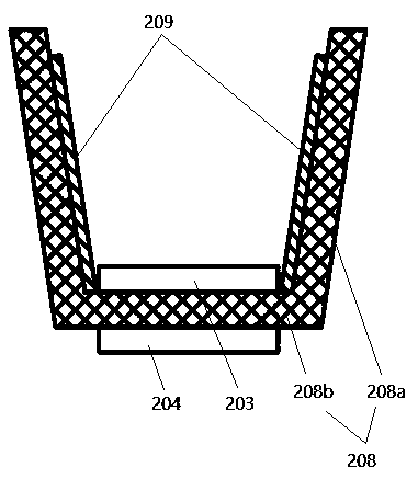
[0026] Example 2, please combine figure 2 and image 3 As shown, the ultraviolet LED packaging structure involved in this embodiment includes a substrate 201 and a light-transmitting housing 202. The light-transmitting housing 202 is made of soda-lime glass, and can be a closed space 207 formed by a cuboid structure with six sides closed. Combination by buckle, riveting, gluing, etc. In addition, the airtight space 207 can be formed by the light-transmitting casing 202 and the substrate 201 , that is, a part of the substrate 201 protrudes from the light-transmitting casing 202 , and the two are sealed and connected. The heat conduction gas is filled in the above-mentioned closed space 207 to enhance heat dissipation. The substrate 201 is used to carry the circuit and the ultraviolet LED chip 203, and the emission wavelength of the ultraviolet LED chip 203 is 10-405nm. A printed circuit is provided on the substrate 201 . The difference from the first embodiment is that the ...
Embodiment 3
[0027] Example 3, please combine Figure 4 As shown, the ultraviolet LED packaging structure involved in this embodiment includes a substrate 301 and a light-transmitting housing 302. The light-transmitting housing 302 is made of borosilicate glass. Combination by buckle, riveting, gluing, etc. In addition, the airtight space 307 can be formed by the light-transmitting casing 302 and the substrate 301 , that is, a part of the substrate 301 protrudes from the light-transmitting casing 302 , and the two are sealed and connected. The heat conduction gas is filled in the above-mentioned closed space 307 to enhance heat dissipation. The substrate 301 is used to carry the circuit and the ultraviolet LED chip 303, and the emission wavelength of the ultraviolet LED chip 303 is 10-405nm. A printed circuit is arranged on the substrate 301. The difference from Embodiment 1 is that the substrate 301 is made of a partially flexible material, and the substrate 301 is bent to form a plural...
PUM
| Property | Measurement | Unit |
|---|---|---|
| Angle | aaaaa | aaaaa |
| Luminous wavelength | aaaaa | aaaaa |
Abstract
Description
Claims
Application Information
 - R&D Engineer
- R&D Manager
- IP Professional
- Industry Leading Data Capabilities
- Powerful AI technology
- Patent DNA Extraction
Browse by: Latest US Patents, China's latest patents, Technical Efficacy Thesaurus, Application Domain, Technology Topic, Popular Technical Reports.
© 2024 PatSnap. All rights reserved.Legal|Privacy policy|Modern Slavery Act Transparency Statement|Sitemap|About US| Contact US: help@patsnap.com


