Cleaning equipment and semiconductor wafer cleaning equipment

A cleaning device and megasonic cleaning technology, which are applied in semiconductor/solid-state device manufacturing, cleaning methods and tools, cleaning methods using liquids, etc., can solve the problems of wafer center structure damage, incomplete cleaning, and low energy density

Active Publication Date: 2021-01-22
BEIJING SEMICORE PRECISION MICROELECTRONICS EQUIP CO LTD
View PDF5 Cites 2 Cited by
  • Summary
  • Abstract
  • Description
  • Claims
  • Application Information

AI Technical Summary

Problems solved by technology

[0003] The purpose of this application is to provide a cleaning device and semiconductor wafer cleaning equipment, which are used to clean the surface of the rotating wafer, which solves the problem that the megasonic cleaning equipment in the prior art has energy at places closer to the edge of the wafer. The lower the density, the less thorough the cleaning; and the concentration of the acoustic wave energy near the center of the wafer will lead to structural damage in the center of the wafer in severe cases, and even technical problems such as pits when cleaning the dielectric layer

Method used


Image

  • Cleaning equipment and semiconductor wafer cleaning equipment
  • Cleaning equipment and semiconductor wafer cleaning equipment
  • Cleaning equipment and semiconductor wafer cleaning equipment

Examples


Embodiment 1

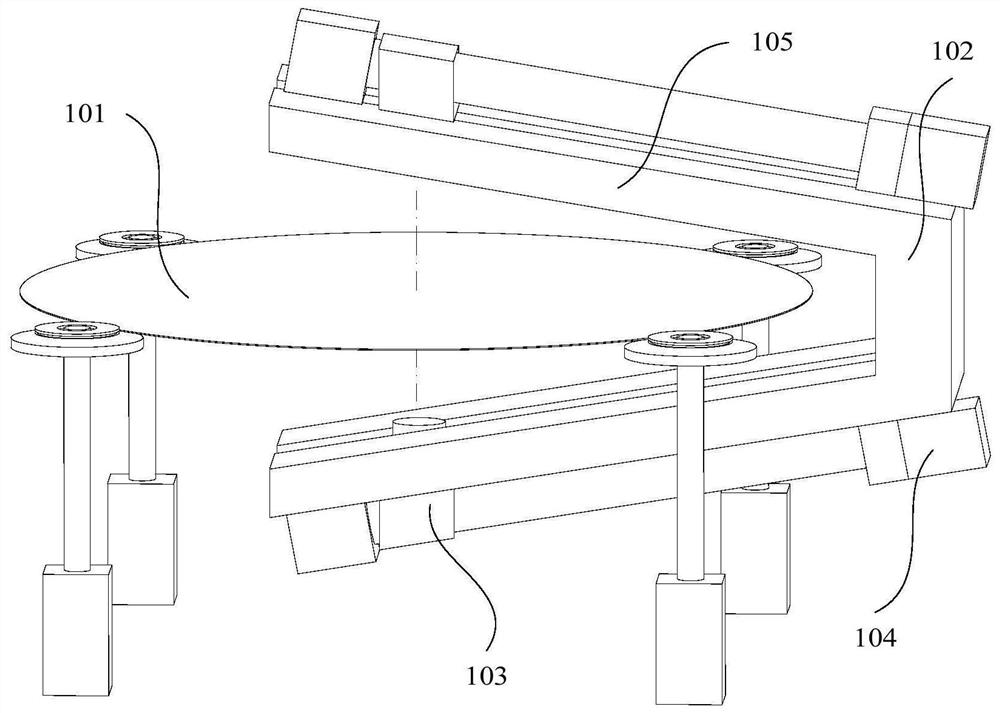
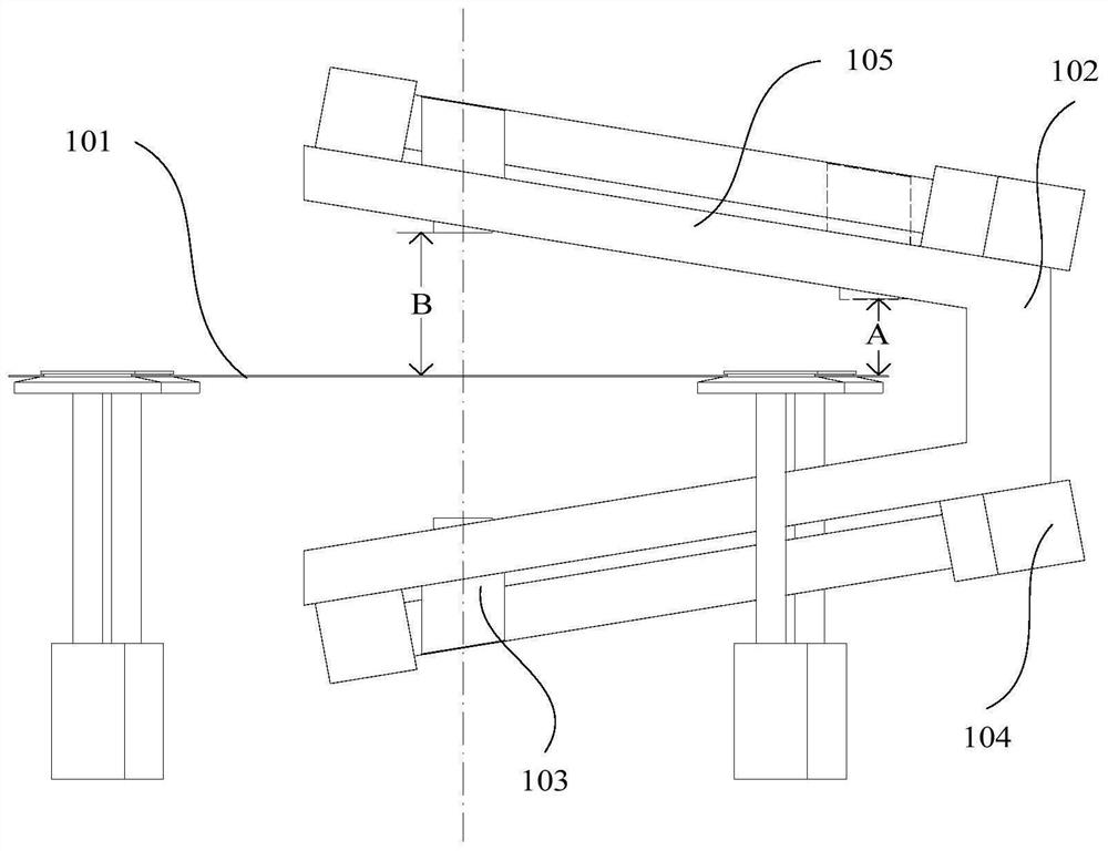
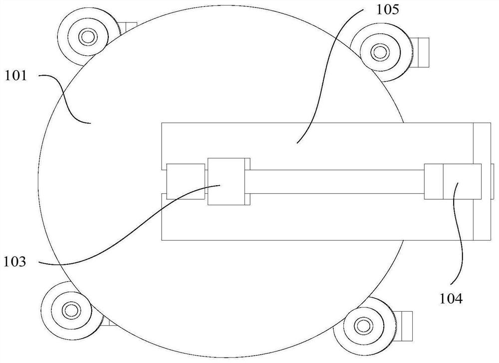
[0032] see Figure 1 to Figure 3 As shown, among them, figure 1 The cleaning device provided for Embodiment 1 of the present application is used to clean the rotating object 101 to be cleaned, including a support frame 102, a megasonic cleaning assembly 103 and a driving device 104; the support frame 102 is provided with a support arm 105, and the megasonic cleaning assembly 103 is located on the support arm 105, and the driving device 104 is used to drive the megasonic cleaning assembly 103 to reciprocate along the length direction of the support arm 105; the megasonic cleaning assembly 103 is used to clean the surface of the object to be cleaned 101; the length direction of the support arm 105 Set at an angle with the surface of the object to be cleaned 101, the vertical distance between the starting point of the movement of the megasonic cleaning assembly 103 and the surface of the object to be cleaned 101 is smaller than the distance between the end point of the movement o...

Embodiment 2

[0043] The cleaning device in the second embodiment is an improvement on the basis of the above embodiment. The technical content disclosed in the above embodiment will not be described repeatedly, and the content disclosed in the above embodiment also belongs to the content disclosed in the second embodiment.

[0044] see Figure 4 As shown, in the optional scheme of this embodiment, the megasonic cleaning assembly 103 includes a megasonic cleaning nozzle 107 and a liquid inlet pipe 108, and the liquid inlet pipe 108 is communicated with the megasonic cleaning nozzle 107, and the liquid inlet pipe 108 is used for cleaning The liquid is transported to the megasonic cleaning nozzle 107.

[0045] In this embodiment, the megasonic cleaning assembly 103 includes a megasonic cleaning nozzle 107 and a liquid inlet pipe 108, and the liquid inlet pipe 108 can transport the cleaning liquid to the megasonic cleaning nozzle 107, so that the sound waves can be combined with the chemical r...

Embodiment 3

[0054] Embodiment 3 of the present application provides a semiconductor wafer cleaning device, which includes the cleaning device described in any of the above embodiments, and thus has all the beneficial technical effects of the cleaning device described in any of the above embodiments. Here, no Let me repeat.


PUM


Abstract

The invention relates to the technical field of semiconductor cleaning, in particular to a cleaning device and semiconductor wafer cleaning equipment. The cleaning device comprises a supporting frame,a megasonic cleaning assembly and a driving device; a supporting arm is arranged on the supporting frame; the megasonic cleaning assembly is located on the supporting arm; the driving device is usedfor driving the megasonic cleaning assembly to do a reciprocating motion in a length direction of the supporting arm; an angle is formed between the length direction of the supporting arm and the surface of a to-be-cleaned object; and a vertical distance between a motion starting point of the megasonic cleaning assembly and the surface of the to-be-cleaned object is smaller than a vertical distance between a motion end point of the megasonic cleaning assembly and the surface of the to-be-cleaned object. The cleaning device disclosed by the invention solves the technical problems of incompletecleaning of the megasonic cleaning equipment due to lower energy density in a position closer to the edge of a wafer, wafer center structure damage caused by serious acoustic wave energy concentrationin a position close to the center of the wafer, and even pits generated in cleaning a dielectric layer.

Description

technical field [0001] The present application relates to the technical field of semiconductor cleaning, in particular to a cleaning device and semiconductor wafer cleaning equipment. Background technique [0002] After the CMP (Chemical Mechanical Polishing, chemical mechanical polishing) process, various pollutants such as organic compounds, particles and metal ions will remain on the surface of the wafer. After the CMP process, ultrasonic or megasonic cleaning technology is used in the wafer cleaning process It can effectively remove impurity pollution. In the existing ultrasonic or megasonic cleaning technology, the acoustic wave generator sweeps from the edge of the rotating wafer to the center of the wafer at a uniform speed. The closer to the edge of the wafer, the lower the energy density, and the cleaning is not thorough; The energy of the acoustic wave in the center is concentrated, and in severe cases, it will cause damage to the structure of the wafer center, an...

Claims


Application Information

Patent Timeline
Patent Type & Authority Patents(China)
IPC IPC(8): H01L21/67B08B3/02
CPCB08B3/024B08B2203/0288H01L21/67051
Inventor 赵宁史霄尹影佀海燕
Owner BEIJING SEMICORE PRECISION MICROELECTRONICS EQUIP CO LTD
Why Eureka
Try Eureka