Preparation method of graphene monocrystal

A graphene and single crystal technology, applied in the field of graphene single crystal preparation, can solve the problem of low efficiency of graphene single crystal preparation

Inactive Publication Date: 2019-02-12
INST OF MICROELECTRONICS CHINESE ACAD OF SCI
View PDF5 Cites 1 Cited by
  • Summary
  • Abstract
  • Description
  • Claims
  • Application Information

AI Technical Summary

Problems solved by technology

[0004] In view of the problems existing in the prior art, the embodiment of the present invention provides a method for preparing a graphene single crystal, which is used to solve the technical problem of low preparation efficiency of graphene single crystal in the prior art

Method used


Image

  • Preparation method of graphene monocrystal
  • Preparation method of graphene monocrystal

Examples


Embodiment 1

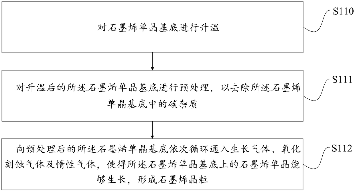
[0026] The present embodiment provides a kind of preparation method of graphene single crystal, such as figure 1 As shown, the methods include:

[0027] S110, heating the graphene single crystal substrate;

[0028] In this embodiment, first determine the material of the graphene single crystal substrate, the graphene single crystal substrate can include: copper Cu substrate, nickel Ni substrate, platinum Pt substrate, silicon Si substrate, germanium Ge substrate, silicon dioxide SiO 2 Any one of the substrate, the sapphire Sapphire substrate, and the zinc oxide ZnO substrate may also be any one or more alloy substrates of Cu, Ni, Pt, Si, and Ge. Preferably, it is a Cu substrate.

[0029] After confirming, put the graphene single crystal substrate into a chemical vapor deposition chamber (CVD, Chemical VaporDeposition), heat up the graphene single crystal substrate, and raise the temperature of the graphene single crystal substrate to 600-1083°C, preferably The ground is 800...

Embodiment 2

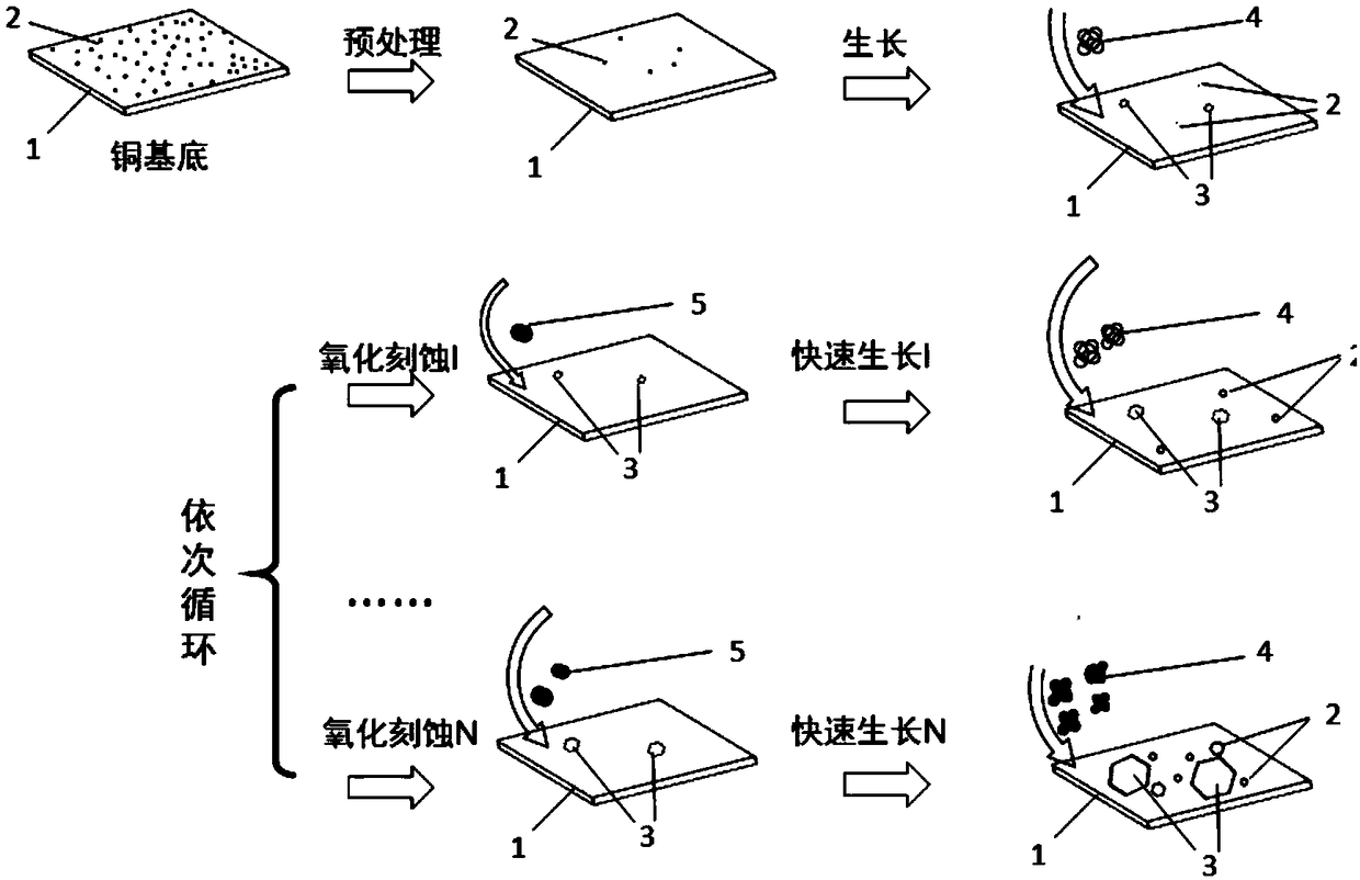
[0043] In practical applications, when a copper substrate is used to prepare a graphene single crystal, the specific implementation is as follows:

[0044] Put the graphene single crystal substrate 1 into the CVD chamber, raise the temperature of the graphene single crystal substrate, and raise the temperature of the graphene single crystal substrate to 750°C. Wherein, the air pressure in the CVD chamber is normal pressure: 720 Torr.

[0045] see figure 2 , pretreating the heated graphene single crystal substrate to remove carbon impurities 2 in the graphene single crystal substrate and reduce the nucleation density of graphene.

[0046] The pretreatment of the heated graphene single crystal substrate includes: annealing the heated graphene single crystal substrate in an oxidizing gas, a reducing gas or an inert gas. Wherein, the oxidizing gas may include: O 2 Mixed gas with Ar, the reducing gas can include H 2 A mixed gas with Ar, the inert gas may include: argon Ar.

...


PUM


Abstract

The invention provides a preparation method of a graphene monocrystal. The preparation method comprises the following steps: heating a graphene monocrystal substrate; pretreating the heated graphene monocrystal substrate so as to remove carbon impurities in the graphene monocrystal substrate; successively circularly introducing growth gas, oxidization etching gas and inert gas into the pretreatedgraphene monocrystal substrate, so as to enable the graphene monocrystal on the graphene monocrystal substrate to grow to form graphene crystal grains, wherein when the growth gas and the oxidizationetching gas are successively circularly introduced, the introduction amount of the growth gas and the oxidization etching gas can be gradually increased according to the preset gas increment amount; therefore, in the growth process, the nucleation density of the graphene can be reduced by successively circularly introducing the oxidization etching gas; the introduction amount of the growth gas isgradually increased according to the preset gas increment amount, so that in the growth process of the graphene monocrystal, sufficient growth gas can be provided, and the growth rate of the graphenemonocrystal can be increased.

Description

technical field [0001] The invention belongs to the technical field of graphene preparation, in particular to a method for preparing a graphene single crystal. Background technique [0002] Graphene is a two-dimensional crystalline material composed of carbon atoms with only one atomic thickness. Its excellent properties in electricity, light and mechanical strength make it have many potential applications in electronics, solar cells, sensors and other fields. [0003] Although the demand for graphene is huge, its preparation speed is slow. The conventional chemical vapor deposition (CVD, Chemical Vapor Deposit) growth method takes nearly 20 hours to prepare a centimeter-sized single-crystal graphene film, which seriously restricts the actual production of graphene. in the application. Contents of the invention [0004] Aiming at the problems existing in the prior art, an embodiment of the present invention provides a method for preparing a graphene single crystal, which ...

Claims


Application Information

Patent Timeline
Patent Type & Authority Applications(China)
IPC IPC(8): C30B29/02C30B25/10C30B25/18
CPCC30B25/10C30B25/186C30B29/02
Inventor 卢维尔夏洋赵丽莉
Owner INST OF MICROELECTRONICS CHINESE ACAD OF SCI
Why Eureka
Try Eureka