A UAV electronic chip manufacturing equipment

An electromechanical and chip technology, which is applied in the field of UAV electronic chip manufacturing equipment, can solve the problems of polishing machine interior and chip wafer pollution, lack of grinding waste collection components, increased labor intensity of manual cleaning, etc., to ensure polishing Accuracy, simple structure, and the effect of preventing jamming and excessive wear

Inactive Publication Date: 2020-08-21
北京圣龙缘科技有限公司
View PDF7 Cites 0 Cited by
  • Summary
  • Abstract
  • Description
  • Claims
  • Application Information

AI Technical Summary

Problems solved by technology

[0003] The present invention provides a kind of UAV electronic chip manufacturing equipment, which can effectively solve the problem that the traditional polishing machine proposed in the above-mentioned background technology generally uses a suction cup to absorb a single chip wafer to polish the surface of the chip wafer one by one. As a result, the efficiency of the traditional polishing machine is low. At the same time, in the actual process of the traditional polishing machine, due to the continuous frictional contact between the polishing head and the chip wafer, a large amount of heat may be accumulated on the surface of the chip wafer, and the lack of conductivity Gas heat conduction components make the chip wafer easy to burn due to excessive heat. In addition, the existing polishing machine lacks a collection component for grinding waste during the polishing process, resulting in debris and debris generated during polishing. Dirt, etc. are prone to overflow, which in turn easily causes different degrees of pollution inside the polishing machine and outside the chip wafer, further increasing the labor intensity of manual cleaning.

Method used


Image

  • A UAV electronic chip manufacturing equipment
  • A UAV electronic chip manufacturing equipment
  • A UAV electronic chip manufacturing equipment

Examples


Embodiment

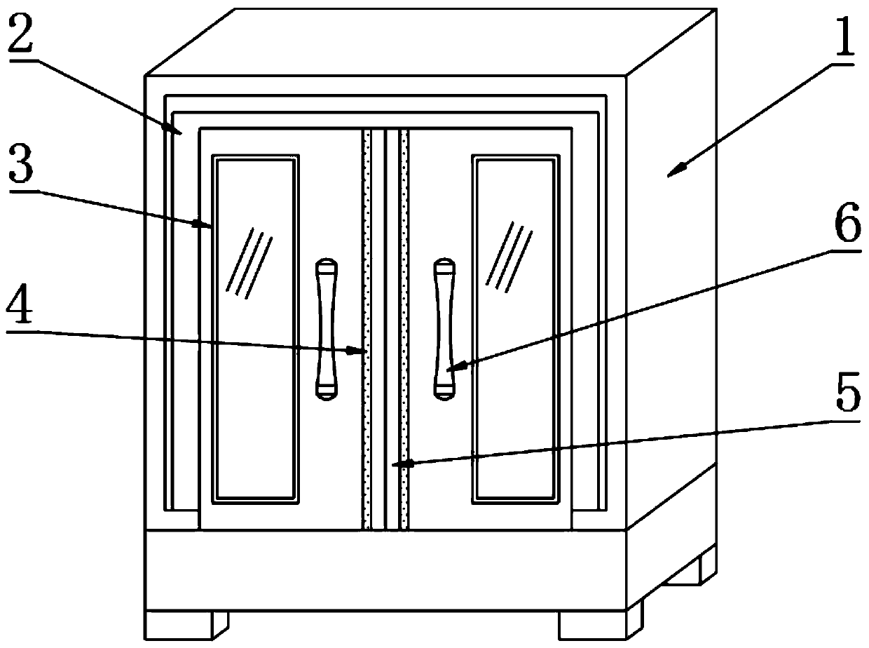
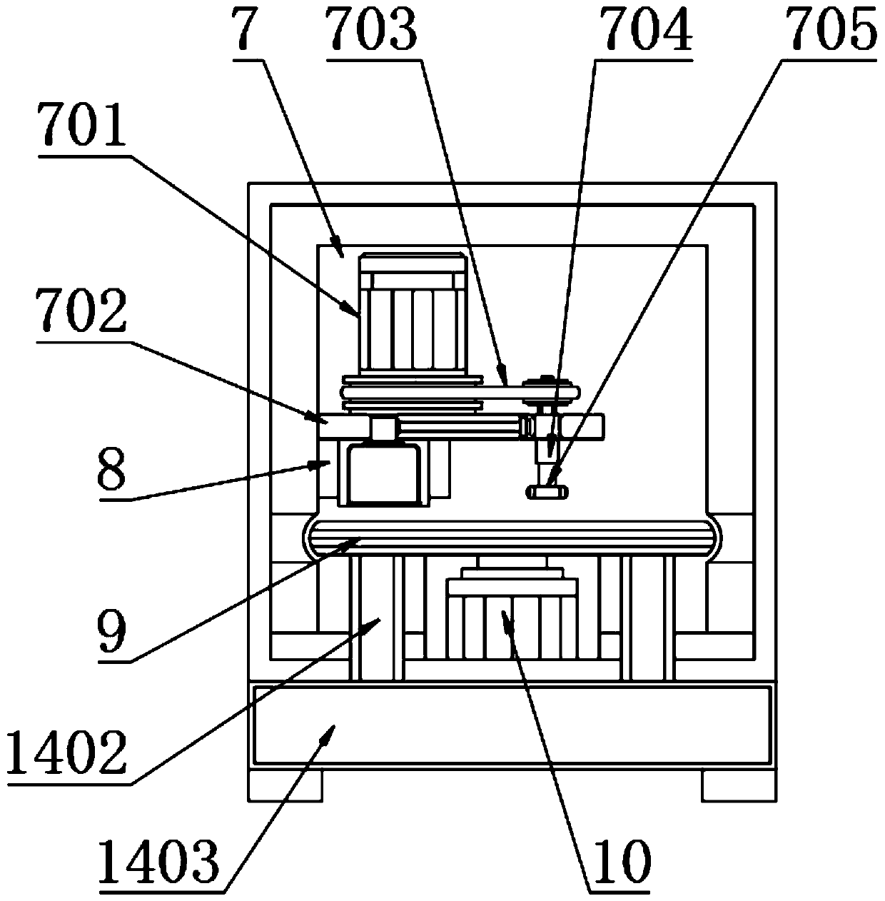
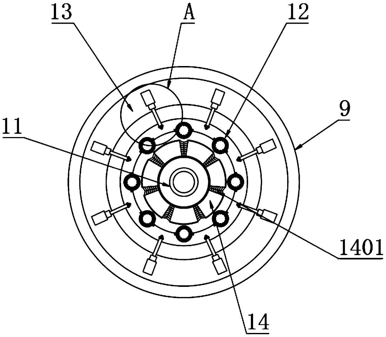
[0030] Example: such as Figure 1-6 As shown, the present invention provides a technical solution, a UAV electronic chip manufacturing equipment, including a polishing body 1, in order to facilitate people to support the polishing body 1, and make the support more stable when supporting the polishing body 1, polishing The bottom of the body 1 is fixedly supported with a support, and the bottom surface of the support is fixedly bonded with a non-slip gasket, and the outer side of the polishing body 1 is rotated with a screen door 3. To observe the polishing efficiency of the wafer, the inner side of the screen door 3 is provided with a perspective window, and the inner side of the screen door 3 is symmetrically provided with a handle 6, and the connection between the screen door 3 and the polishing machine body 1 is provided with a dust-proof rubber layer 2. A sealant edge 4 is bonded to the connection of the inner side of the shielding door 3, and the outside of the sealant ed...


PUM


Abstract

The invention discloses an unmanned aerial vehicle electronic chip manufacturing device which comprises a polishing machine body. A polishing assembly is arranged on the upper part of the inner part of the polishing machine body; a polishing table is annularly arranged on the inner side of a rotary table; an installation groove is formed in the middle of the inner side of the polishing table; a movable disassembling table is fixedly arranged on the bottom part of the inner side of the installation groove; fastening lugs are equidistantly arranged on the inner side edge part of the movable disassembling table; and clamping electromagnets are symmetrically arranged on two side edge parts of the polishing table. The unmanned aerial vehicle electronic chip manufacturing device provided by theinvention is scientific and reasonable in structure and safe and convenient to use; through the components such as the installation groove, the fastening lugs and the clamping electromagnets, chip wafers are conveniently and firmly clamped so as to be prevented from deviating during the polishing process, so that the polishing accuracy of the chip wafers is further ensured; and meanwhile, the chipwafers are clamped through clamping assemblies at multiple stations at the same time, so that the multiple wafers can be polished at the same time, the polishing efficiency of the chip wafers is improved, and the device is simple and convenient to operate.

Description

technical field [0001] The invention relates to the technical field of electronic chips, in particular to a UAV electronic chip manufacturing equipment. Background technique [0002] With the continuous progress of the current society, people use chips more and more frequently, such as drone chips in the prior art, and chips need to be polished by polishing machines many times in the process of mass production. The surface of the chip semi-finished product is polished and polished. For example, after the chip is electroplated, copper ions are deposited on the chip surface to form a thin copper layer. At this time, a polishing machine is required to polish and grind the copper layer on the chip surface. That is to polish the surface of the chip wafer to make the surface of the chip wafer smoother. The traditional polishing machine generally uses a suction cup to absorb a single chip wafer to polish the surface of the chip wafer one by one, resulting in the traditional polishi...

Claims


Application Information

Patent Timeline
Patent Type & Authority Patents(China)
IPC IPC(8): B24B7/22B24B29/02B24B41/06B24B27/00B24B55/06
CPCB24B7/228B24B27/0015B24B29/02B24B41/068B24B55/06
Inventor 王强
Owner 北京圣龙缘科技有限公司
Why Eureka
Try Eureka