
A kind of manufacturing method of one-time molded plastic-encapsulated photocoupler

A technology of optocoupler and manufacturing method, which is applied in the direction of circuits, electrical components, semiconductor devices, etc., can solve problems such as difficult problems, high cost and process, achieve enhanced reflection effect, accurately adjust transmission delay, and improve photoelectric coupling efficiency Effect

Active Publication Date: 2020-01-31
郑州兴航科技有限公司
View PDF4 Cites 0 Cited by
  • Summary
  • Abstract
  • Description
  • Claims
  • Application Information

AI Technical Summary

Problems solved by technology

Therefore, it is necessary to use light-guiding medium molding dies with different cavity shapes or light-guiding mediums with different transparency (changing material components) or metal lead frames with different shapes, whether it is changing the light-guiding medium molding mold, changing the existing metal Making molds for lead frames still requires changing the components of the light-conducting dielectric material, and there are high costs and technical difficulties in the actual production and production process, so the above patented technical solutions have great limitations in use

Method used


Image

  • A kind of manufacturing method of one-time molded plastic-encapsulated photocoupler
  • A kind of manufacturing method of one-time molded plastic-encapsulated photocoupler
  • A kind of manufacturing method of one-time molded plastic-encapsulated photocoupler

Examples


Embodiment Construction

[0041] The patent will be described in further detail below in conjunction with the accompanying drawings, which is an explanation of the present invention rather than a limitation.

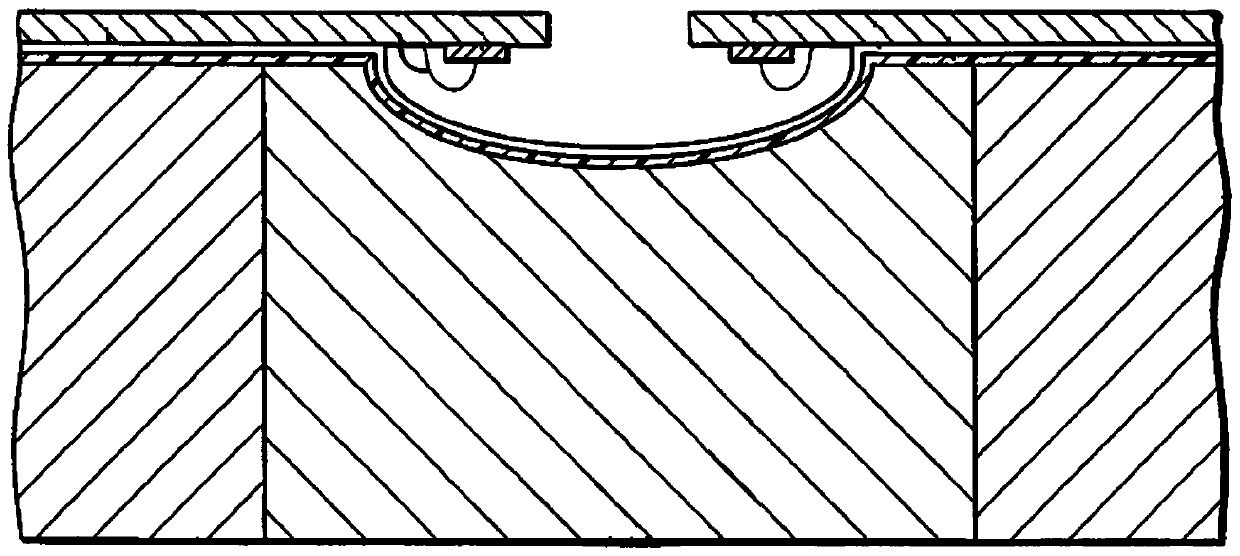
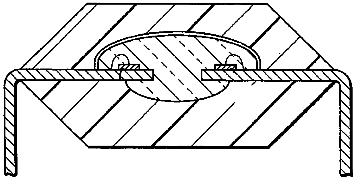
[0042] The traditional coplanar plastic-encapsulated optocoupler adopts multiple molding technology, and the manufacturing process is as follows: Figure 1 ~ Figure 3as shown, figure 1 To make the optical coupler photoconductive medium forming mold for this process, first use conductive glue to bond the light-emitting chip and light-receiving chip of the photocoupler on the surface of the gold island of the tube leg of the metal lead frame, and bond the wire to make the chip and the gold island An electrical connection is formed, and the two gold islands are separated by a certain distance to form electrical isolation. After the photoconductive medium is injected and cured, turn over the photoconductive medium forming mold to form figure 2 The form of the semi-finished product is shown, and th...


PUM


Abstract

The invention discloses a manufacture method for a one-time molded plastic package photoelectric coupler. According to the method, the bearing structure of the plastic package photoelectric coupler ismanufactured; an internal light-guide medium molded structure is designed and formed, so that the photoelectric coupling efficiency of the device can be effectively improved; with various forming molds for changing the shape of the inner cavity of the light-guide medium or doping processes for changing the transparency of the light-guide medium and complicated steps for changing the angle of thegold island of a lead frame not required, the current transfer ratio (CTR) parameter of the photoelectric coupler can be conveniently and accurately adjusted; just by developing a housing injection mold once, the plastic packaging of the photoelectric coupler product and the fine grading of the performance parameters of the photoelectric coupler product can be realized; the photoelectric couplingefficiency of the coplanar optocoupler is optimized; the problem of the coplanar packaging of the fine grading of the current transfer ratio (CTR) of the photoelectric coupler by a one-time injectionmold can be solved; and the plastic packaging of the photoelectric coupler and the precise and controllable product performance parameters of the photoelectric coupler are realized with the development costs of product molds reduced.

Description

technical field [0001] The invention belongs to the field of optoelectronic integrated circuits, and in particular relates to a manufacturing method of a one-time molded plastic-encapsulated photocoupler. Background technique [0002] At present, the international mainstream coplanar plastic-encapsulated optocoupler adopts multiple molding technology. During the production process, in order to form the optical path, it is necessary to perform injection molding of the light-conducting medium. figure 1 For the optical coupler photoconductive medium forming mold of this production method, first use conductive glue to bond the light-emitting chip and light-receiving chip of the photocoupler on the surface of the gold island of the tube leg of the metal lead frame, and the bonding wire makes the chip and the gold The islands form an electrical connection, and two gold islands are separated by a certain distance to form electrical isolation. After the photoconductive medium is in...

Claims


Application Information

Patent Timeline
Patent Type & Authority Patents(China)
IPC IPC(8): H01L31/12H01L31/0203
CPCH01L31/0203H01L31/125
Inventor 陈斌张丰王普昌崔祖石王雷
Owner 郑州兴航科技有限公司
Learn More