
Stacked embedded package structure and manufacturing method thereof

A packaging structure and embedded technology, which is applied in semiconductor/solid-state device manufacturing, electrical components, electric solid-state devices, etc., can solve problems that hinder the development of miniaturization of semiconductor packaging device assembly, docking standards and complicated processes, and insufficient precision. Achieve high integration, realize miniaturization, and reduce the effect of circulation and transfer

Pending Publication Date: 2019-02-01
浙江熔城半导体有限公司
View PDF0 Cites 6 Cited by
  • Summary
  • Abstract
  • Description
  • Claims
  • Application Information

AI Technical Summary

Problems solved by technology

[0006] The disadvantages of the above-mentioned existing processes are: (1) the docking standards and processes between the semiconductor electronic package and the semiconductor package device are complex and cumbersome; (2) on the surface mount, the semiconductor package device is usually connected by solder Electrical interconnection with the circuit board; (3) The current surface mount solder connection requires a large pad and pad spacing of the semiconductor package device, such as the pad / spacing is 280 microns / 400 microns, which is not precise enough, and the solder The connection requires more complex solder reflow process control; (4) The semiconductor packaging device is assembled on the circuit board by surface mount method. Due to the increase in the area of ​​the semiconductor packaging device, it will occupy a larger surface area of ​​the circuit board, hindering the semiconductor package. Miniaturization of packaged device assembly

Method used


Image

  • Stacked embedded package structure and manufacturing method thereof
  • Stacked embedded package structure and manufacturing method thereof
  • Stacked embedded package structure and manufacturing method thereof

Examples


Embodiment Construction

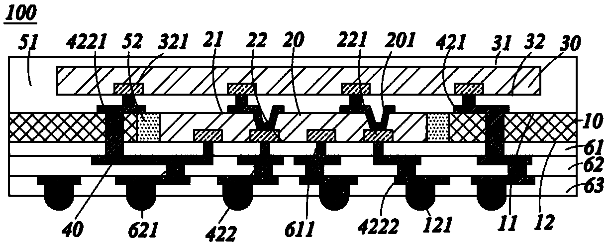
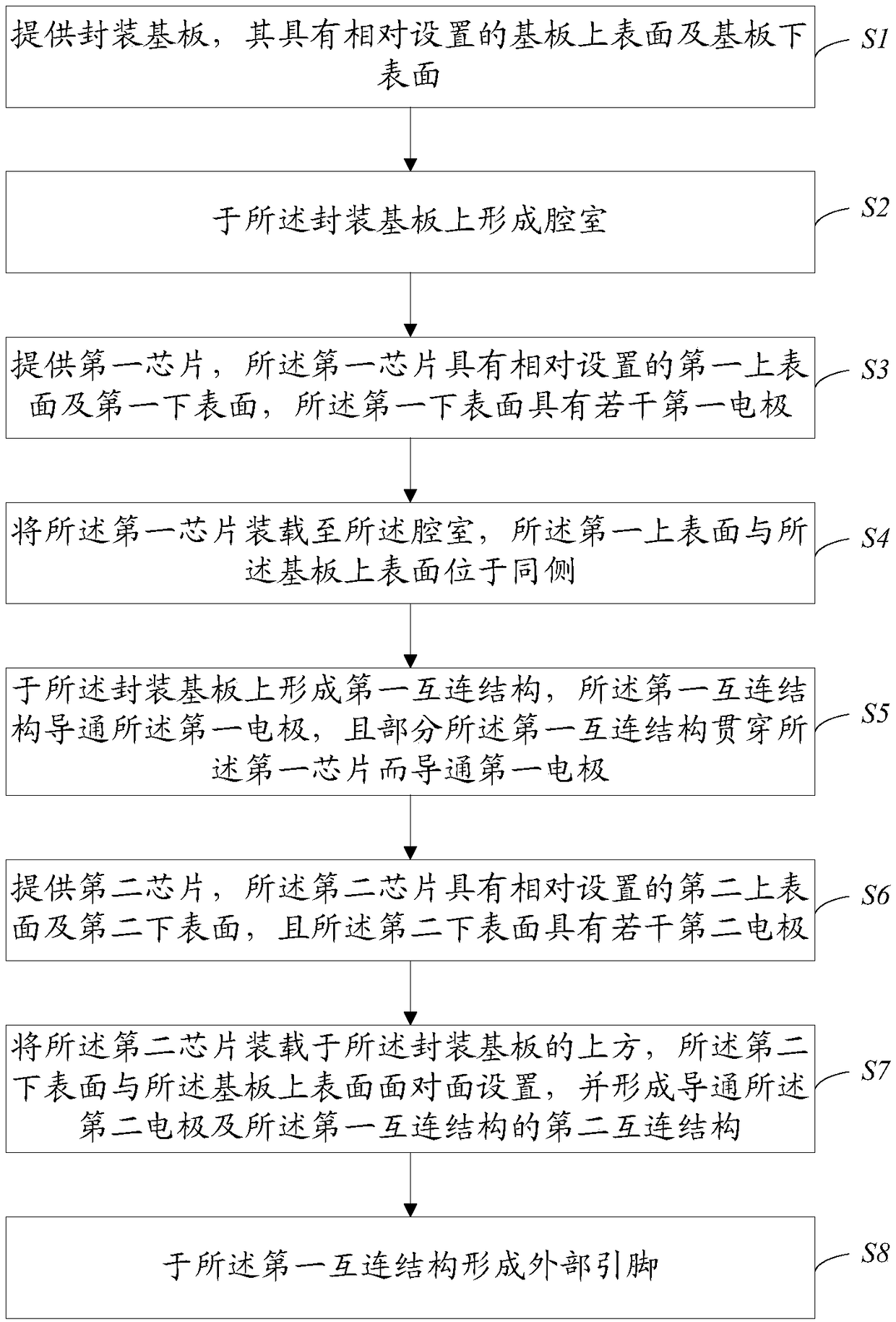
[0053] The present invention will be described in detail below in conjunction with the specific embodiments shown in the drawings. However, these embodiments do not limit the present invention, and the structural, method, or functional changes made by those skilled in the art based on these embodiments are all included in the protection scope of the present invention.

[0054] In each figure of the present application, for the convenience of illustration, some dimensions of the structure or part will be exaggerated relative to other structures or parts, therefore, only used to illustrate the basic structure of the subject of the present application.

[0055] In addition, terms such as "upper", "above", "below", "below" and the like used herein to indicate a relative position in space are for ease of explanation to describe a unit or feature as shown in the drawings relative to The relationship of another unit or feature. The term of the relative position in space may be intended t...


PUM


Abstract

The present invention discloses a stacked embedded package structure and a manufacturing method thereof. The package structure includes a package substrate, a first chip, a second chip, and a plurality of interconnection structures; the package substrate is provided with an upper substrate surface and a lower substrate surface which are arranged oppositely; the package substrate has a chamber; thefirst chip is disposed in the chamber; the first lower surface of the first chip is provided with a plurality of first electrodes; the second chip is disposed on the package substrate; the second lower surface of the second chip is provided with a plurality of second electrodes; the plurality of interconnection structures are used for conductively connecting the plurality of first electrodes andthe plurality of second electrodes; and a part of the interconnection structures pass through the first chip so as to conductively connect the first electrodes. According to the stacked embedded package structure and the manufacturing method thereof of the invention, the packaging technology is utilized to package the two different chips on the same package substrate, and therefore, multi-chip high integration can be realized, and the utilization ratio of the package substrate can be improved; and the packaging processing of semiconductor chip packaging and a semiconductor package body is completed at the package substrate, and therefore, complicated and cumbersome standards and process docking of the semiconductor chip packaging and the semiconductor package body can be omitted, the circulation and transfer of electronic manufacturing can be decreased, manpower and material resources can be saved, and the cost of electronic products can be further reduced.

Description

Technical field [0001] The invention relates to the field of semiconductor packaging, in particular to a stacked embedded packaging structure and a manufacturing method thereof. Background technique [0002] Stacked semiconductor chip packaging is an important 3D packaging form to realize miniature high-density system-in-a-package, which is beneficial to improve the package integration and package device performance. [0003] Currently, the industry has the following main structures and process methods to realize stacked chip interconnection: [0004] (1) First complete the multi-layer stacking of bare chips, and then perform related multi-chip electrical interconnection by means of leads to complete the basic stacked chip system interconnection; [0005] (2) The assembly of semiconductor packaged devices on circuit boards is usually completed by surface mount technology. [0006] The shortcomings of the above-mentioned existing processes are: (1) The docking standards and processes be...

Claims


Application Information

Patent Timeline
Patent Type & Authority Applications(China)
IPC IPC(8): H01L25/065H01L23/538H01L21/50
CPCH01L23/5384H01L23/5386H01L25/0657H01L21/50H01L2225/06555H01L2225/06506H01L2924/181H01L2924/15311H01L2224/16225H01L2224/18H01L2924/00012
Inventor 蔡亲佳
Owner 浙江熔城半导体有限公司
Learn More