


Quick Research
Generate reliable direction feasibility study reports for your R&D in just a few steps.

Technical Q&A
Discover and master advanced knowledge NOW. Basics, ideas, possibilities, all at once.

Find Solutions
As an expert in R&D theories, this can generate solutions to your technical problems instantly.

Evaluate Feasibility
Analyze your overall solution with one click, know your potential R&D risks in advance.

Monitor Landscape
Get weekly tech updates, stay abreast of the latest tech innovations and key insights.
A Millimeter Wave Linearization Method Based on Schottky Diode
A Schottky diode, millimeter wave technology, applied in the field of radio frequency, can solve the problems of complex linearization technology structure, difficult to exert the best effect, low linearity compensation, etc., to improve integration and working speed, nonlinear distortion Improve and enhance the effect of linearity compensation
- Summary
- Abstract
- Description
- Claims
- Application Information
AI Technical Summary
Problems solved by technology
Method used
Image

Examples
Embodiment 1
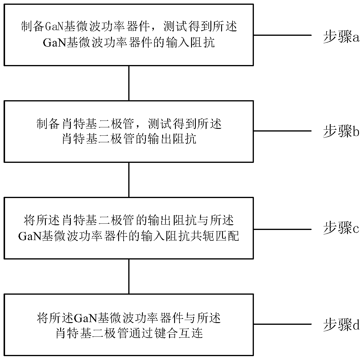
[0052] See figure 1 , figure 1 It is a schematic flowchart of a Schottky diode-based millimeter wave linearization method provided by an embodiment of the present invention. The preparation method specifically comprises the following steps:
[0053] Step a, preparing a GaN-based microwave power device, and testing to obtain the input impedance of the GaN-based microwave power device;
[0054] Step b, preparing a Schottky diode, and testing to obtain the output impedance of the Schottky diode;
[0055] Step c, conjugate matching the output impedance of the Schottky diode with the input impedance of the GaN-based microwave power device;
[0056]Step d, interconnecting the GaN-based microwave power device and the Schottky diode through bonding.
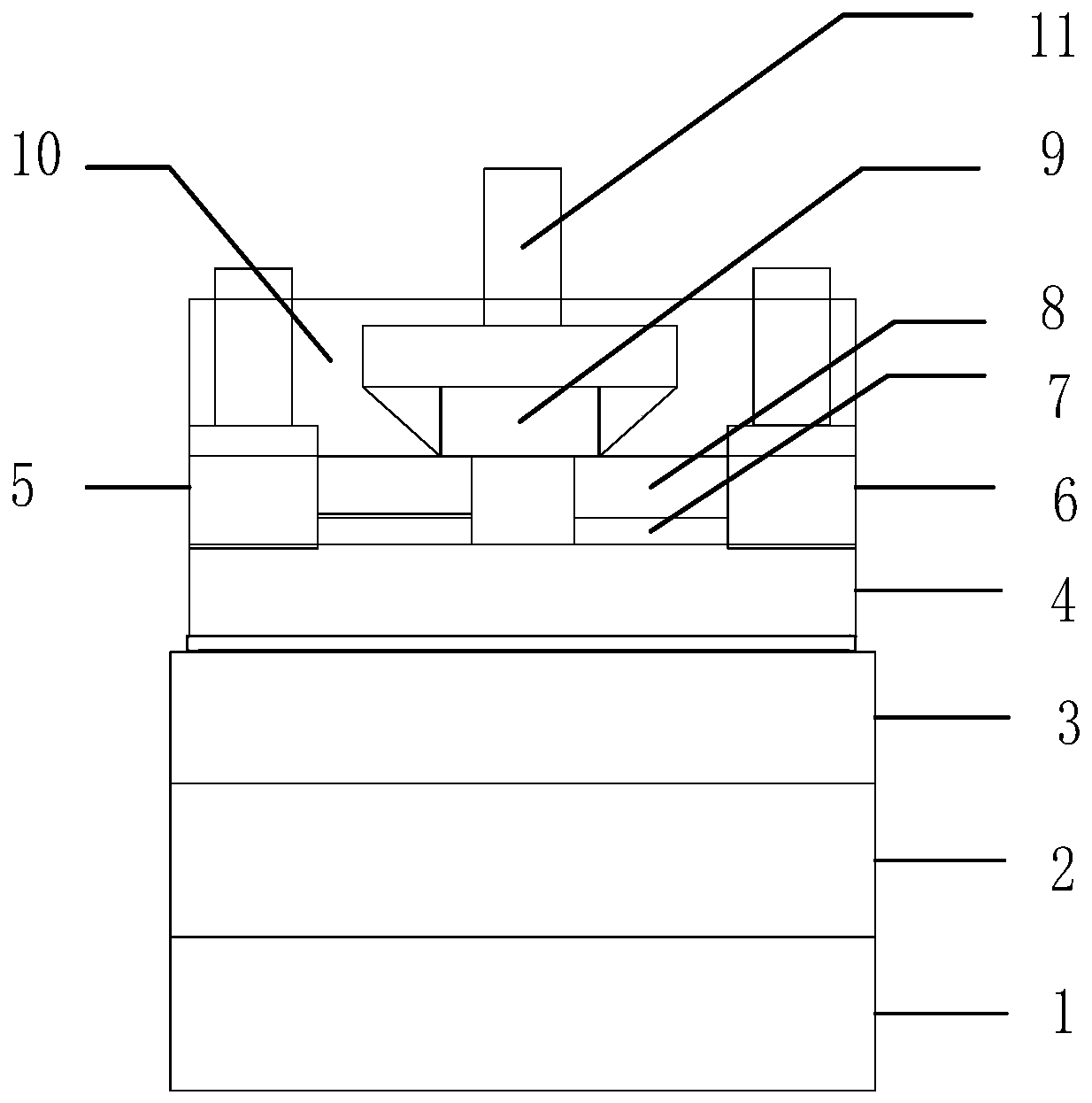
[0057] Further, see figure 2 , figure 2 A schematic diagram of a three-dimensional structure of a GaN-based microwave power device with low frequency loss provided by an embodiment of the present invention. The preparation metho...
Embodiment 2
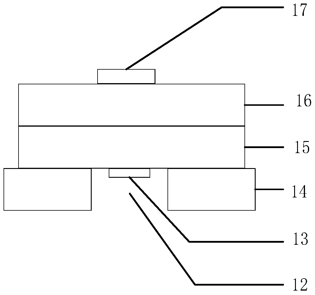
[0153] See Figure 4 , Figure 4 A schematic diagram of a three-dimensional structure after bonding a Schottky diode and a GaN-based microwave power device provided by an embodiment of the present invention. In this embodiment, on the basis of the foregoing embodiments, a Schottky diode-based millimeter wave linearization method of the present invention will be described in detail. Specifically, the method may include:
[0154] Low-frequency loss GaN-based microwave power devices use SiC substrates, AlGaN / GaN HEMTs with a gate width of 100 μm and a gate length of 0.1 μm, and vertical structure Schottky diodes use W as the Schottky metal.
[0155] The device is manufactured on the purchased epitaxial substrate sample which already contains substrate, nucleation layer, buffer layer and potential barrier layer.
[0156] Step 1, cleaning the epitaxial substrate sample.
[0157] First place the sample in acetone and sonicate for 2 minutes, then boil it for 10 minutes in a posit...
PUM
| Property | Measurement | Unit |
|---|---|---|
| thickness | aaaaa | aaaaa |
| thickness | aaaaa | aaaaa |
| width | aaaaa | aaaaa |
Abstract
Description
Claims
Application Information
 - R&D Engineer
- R&D Manager
- IP Professional
- Industry Leading Data Capabilities
- Powerful AI technology
- Patent DNA Extraction
Browse by: Latest US Patents, China's latest patents, Technical Efficacy Thesaurus, Application Domain, Technology Topic, Popular Technical Reports.
© 2024 PatSnap. All rights reserved.Legal|Privacy policy|Modern Slavery Act Transparency Statement|Sitemap|About US| Contact US: help@patsnap.com