Optical module connecting finger cut-off position anti-electroplating ink pattern structure

A graphic structure and anti-plating technology, applied in electrical components, printed circuits, printed circuits, etc., can solve the problems of gold finger penetration, ink shedding, and dirty etching, etc., to reduce shedding, reduce production costs, and improve etching leads Effect

Pending Publication Date: 2019-01-11
深圳欣强智创电路板有限公司
View PDF1 Cites 3 Cited by
  • Summary
  • Abstract
  • Description
  • Claims
  • Application Information

AI Technical Summary

Problems solved by technology

[0005] However, the production and processing process of the cut-off gold finger is very different from that of the ordinary gold finger. The cut-off gold finger is strictly controlled during processing, and the industry standard design is 0.1+ / -0.05 mm, because the line spacing is too small, when making anti-plating ink, it is easy to cause the ink to fall off, resulting in gold seepage in the position of the gold finger after electroplating, and the etching is not clean and scrapped

Method used


Image

  • Optical module connecting finger cut-off position anti-electroplating ink pattern structure

Examples


Embodiment

[0020] Example: refer to figure 1 .

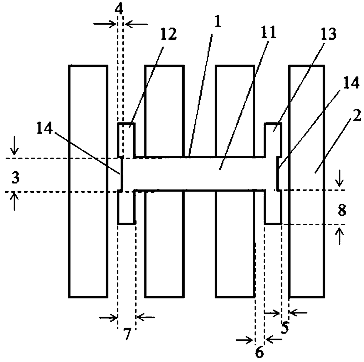
[0021] An anti-plating ink graphic structure of a truncated position of an optical module gold finger, which includes an anti-plating ink 1, and the anti-plating ink 1 is arranged on the truncated position of the gold finger 2; the anti-plating ink 1 is H-shaped, including a waist 11, The left part 12 and the right part 13, the left part 12 and the right part 13 are connected by the waist part 11, the waist part 11 is arranged on the cut-off position of the golden finger 2, and the left part 12 and the right part 13 are arranged at the distance between the golden fingers 2 Above, the left part 12 and the right part 13 of the electroplating ink 1 are provided with grooves 14 for improving the development ability of the electroplating ink 11 . Set the H-type anti-plating ink 1 at the truncated position of the gold finger 2, so that the anti-plating ink 1 is not easy to fall off and deviate from the upper plate, and the design of the groove ...


PUM


Abstract

A cut-off position anti-electroplating ink pattern structure of a connecting finger of an optical module comprises an anti-electroplating ink, wherein the anti-electroplating ink is arranged on the cut-off position of the connecting finger; Characterized by. The anti-electroplating ink is H-shaped and comprises a waist, a left part and a right part, wherein the left part and the right part are connected through the waist, the waist part is arranged at the cut position of the connecting finger, the left part and the right part are arranged at the spacing between the connecting finges, and the left part and the right part of the anti-electroplating ink are provided with grooves for improving the anti-electroplating ink developing ability. The invention utilizes H-type anti-electroplating inkpattern structure, the developing ability of the developing solution is improved. The invention reduces the abnormality of electroplating ink shedding and gold infiltration in the production and processing process of the cut connecting finger, improves the etching lead wire, solves the short circuit at the cut place of the connecting finger caused by the abnormality of the etching, improves the production yield of the product, and has simple design and good use effect.

Description

technical field [0001] The invention relates to the field of printed circuit boards, in particular to an anti-plating ink graphic structure at the truncation position of an optical module golden finger. Background technique [0002] On the printed circuit board near the edge of the board, there are many rectangular metal contacts arranged in rows, and the metal contacts are formed by electroplating a layer of nickel gold on the copper surface of the printed circuit board. These metal contacts are part of the printed circuit board and are called gold fingers because of their nickel-gold-plated surface and their shape resembling fingers. [0003] With the rapid development of electronic technology applications and the improvement of signal integrity requirements, the slot with gold fingers has also broken through the original design method, thus evolving into a segmented gold finger design. The segmented gold finger design is conducive to improving the transmission of high-fr...

Claims


Application Information

Patent Timeline
Patent Type & Authority Applications(China)
IPC IPC(8): H05K1/11
CPCH05K1/117H05K2201/09281
Inventor 殷大望宋国伟
Owner 深圳欣强智创电路板有限公司
Why Eureka
Try Eureka