
A multi-fpga interconnection device

A bus interconnection and AXI technology, applied in the field of solid-state hard drives, can solve the problems of difficult timing convergence, poor flexibility, and high price

Active Publication Date: 2020-07-07
SHENZHEN YILIAN INFORMATION SYST CO LTD
View PDF7 Cites 0 Cited by
  • Summary
  • Abstract
  • Description
  • Claims
  • Application Information

AI Technical Summary

Problems solved by technology

[0002] SSD (Solid State Drives, Solid State Drives) SOC (analog core, System-on-a-Chip) chip verification, due to the limitations of EDA (Electronics Design Automation) prototype verification, generally use FPGA (on-site Programmable Gate Array, Field-Programmable Gate Array) prototype verification, conditional hardware acceleration emulator will also be used, because the current SOC chip scale is very large, the FPGA prototype is to use ASIC (Application Specific Integrated Circuit, Application Specific Integrated Circuit) Logic design conversion is put into FPGA for verification. Although the scale of FPGA is also increasing, there will still be designs where one FPGA cannot accommodate the entire SOC chip. Choosing an FPGA with as large resources as possible is expensive and takes a long time for each synthesis. It needs to be planned, otherwise the timing is difficult to converge and the flexibility is poor. The second is to choose an FPGA with a high-speed transceiver. The disadvantage is that it is expensive and has poor flexibility.

Method used


Image

  • A multi-fpga interconnection device

Examples


Embodiment Construction

[0018] The following will clearly and completely describe the technical solutions in the embodiments of the present invention with reference to the accompanying drawings in the embodiments of the present invention. Obviously, the described embodiments are some of the embodiments of the present invention, but not all of them. Based on the embodiments of the present invention, all other embodiments obtained by persons of ordinary skill in the art without making creative efforts belong to the protection scope of the present invention.

[0019] It should be understood that when used in this specification and the appended claims, the terms "comprising" and "comprises" indicate the presence of described features, integers, steps, operations, elements and / or components, but do not exclude one or Presence or addition of multiple other features, integers, steps, operations, elements, components and / or collections thereof.

[0020] It should also be understood that the terminology used ...


PUM


Abstract

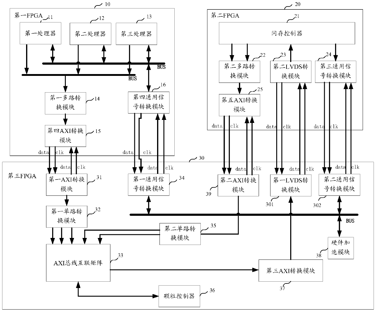
The invention relates to a multi-FPGA interconnecting device and a data transmission method thereof. The device comprises a first FPGA, a second FPGA and a third FPGA. The third FPGA is provided withan AXI bus interconnection matrix, wherein the AXI bus interconnection matrix comprises an AXI bus with multiple inputs and outputs interconnected, and a central processor and a flash memory controller are respectively connected with the AXI bus interconnection matrix through an LVDS interface. As the whole SOC chip design is reasonably divided and placed into a plurality of FPGA, the LVDS interface is adopted for high-speed data transmission by the plurality of FPGAs, the whole device can be synthesized with high speed, the timing is easy to converge, the main function of the SOC chip is realized, the cost is low, and the flexibility is strong.

Description

technical field [0001] The invention relates to a solid-state hard disk, and more specifically refers to a multi-FPGA interconnection device. Background technique [0002] SSD (Solid State Drives, Solid State Drives) SOC (analog core, System-on-a-Chip) chip verification, due to the limitations of EDA (Electronics Design Automation) prototype verification, generally use FPGA (on-site Programmable Gate Array, Field-Programmable Gate Array) prototype verification, conditional hardware acceleration emulator will also be used, because the current SOC chip scale is very large, the FPGA prototype is to use ASIC (Application Specific Integrated Circuit, Application Specific Integrated Circuit) Logic design conversion is put into FPGA for verification. Although the scale of FPGA is also increasing, there will still be designs where one FPGA cannot accommodate the entire SOC chip. Choosing an FPGA with as large resources as possible is expensive and takes a long time for each synthesi...

Claims


Application Information

Patent Timeline
Patent Type & Authority Patents(China)
IPC IPC(8): G06F13/40
CPCG06F13/4068
Inventor 李湘锦张鹏董怀玉王宏伟
Owner SHENZHEN YILIAN INFORMATION SYST CO LTD
Learn More