
A flexible board for easily assembling a circuit board and an assembly fixture thereof

A technology for assembling fixtures and circuit boards, applied in the field of optical communication, can solve problems such as damage to optoelectronic devices and communication modules, product damage, flexible board damage, etc., to improve reliability and yield, protect connection lines, and reduce disconnection. effect of risk

Inactive Publication Date: 2018-12-21
WUHAN BAIQI TECH CO LTD
View PDF5 Cites 0 Cited by
  • Summary
  • Abstract
  • Description
  • Claims
  • Application Information

AI Technical Summary

Problems solved by technology

The high-speed signal pads on the existing flexible board circuit are designed in a row. Due to the concentrated stress at the soldering point, the line of the high-speed signal pad is easy to break, and the corresponding high-speed signal line of the motherboard is difficult to achieve equal length, reducing signal integrity
[0003] And because the flexibility of multi-layer boards is much lower than that of single-layer boards, in the multi-process production and testing of optoelectronic devices and modules, repeated positioning and assembly will cause damage to flexible boards, which not only affects appearance, but also affects performance, leading to the use of flexible boards. Board products must be replaced with new flexible boards at high temperatures before they are sold. During the high temperature replacement process, it is easy to cause damage to the product again and cause it to fail.
Due to the above defects in flexible boards with high-density pads and their press-fitting methods, optoelectronic devices and communication modules are damaged or fail during the manufacturing and testing process, and the defect rate increases

Method used


Image

  • A flexible board for easily assembling a circuit board and an assembly fixture thereof
  • A flexible board for easily assembling a circuit board and an assembly fixture thereof
  • A flexible board for easily assembling a circuit board and an assembly fixture thereof

Examples


Embodiment Construction

[0031] The principles and features of the present invention are described below in conjunction with the accompanying drawings, and the examples given are only used to explain the present invention, and are not intended to limit the scope of the present invention.

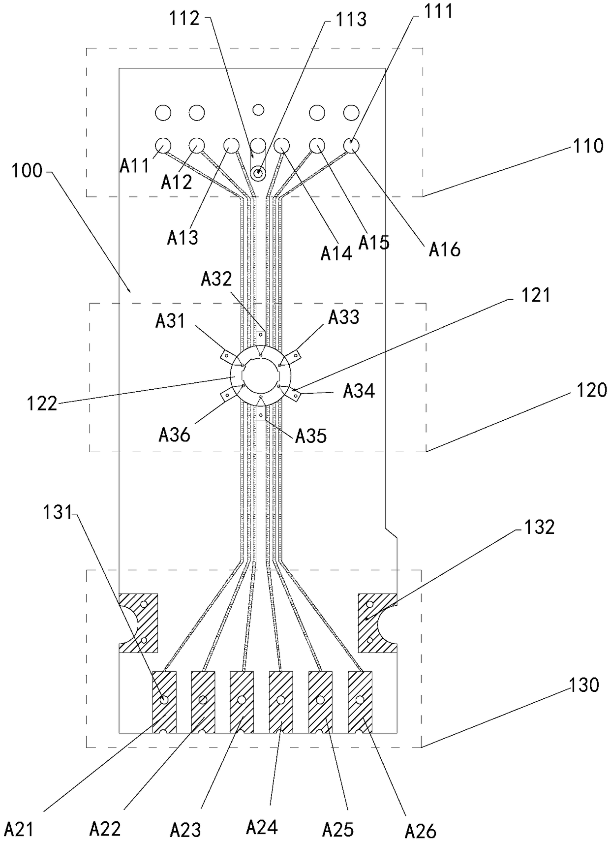
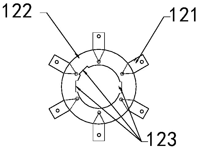
[0032] like figure 1 As shown, a flexible soft board that is easy to assemble a circuit board includes a flexible soft board body 100, on which a main via hole area 110 and a standard pad area 130 are arranged, and in the main pass In the hole area 110, a set of main vias 111 corresponding to the electrical network and the electrical network of the optical device pin to be manufactured or tested is provided. The electrical network corresponds to the standard pad 131 one by one; the standard pad 131 complies with industry standards.

[0033] In the center of the lower end of the main via area 110, an extended pad 112 is longitudinally provided, one end of the extended pad 112 is connected to the main via hole 111, a...


PUM


Abstract

The invention relates to a flexible board for easily assembling a circuit board and an assembling fixture thereof, The flexible board comprises a flexible board body, A main via region and a standardpad region are arrange on the flexible board body, a group of electrical networks correspond to the electrical networks of optical device pins to be fabricated or tested is arranged in the main via region, and a group of standard pads correspond to the electrical networks of the main via are arranged in the standard pad region. The flexible board body further comprises a test pad region, wherein the test pad region is arranged between the main via region and the standard pad region; A set of test pads corresponding to the standard pad electrical network is provided in the test pad area. The invention has the beneficial effects that by increasing the docking tolerance between the pad of the circuit board and the test pad, the poor docking or even misalignment of the pad of the flexible softboard and the circuit board is not easy to occur when the test is carried out, so that the reliability and the yield of the optical device in the test process are improved.

Description

technical field [0001] The invention relates to the technical field of optical communication, in particular to a flexible soft board which is easy to assemble a circuit board and an assembly fixture thereof. Background technique [0002] Flexible board not only has excellent mechanical properties, but also has excellent electrical properties. Flexible boards can be moved, bent, and twisted without damaging the wires, and can have different shapes and special package sizes. Today, as the transmission rate of optical communication is getting higher and higher, the traditional product design can no longer meet the needs of high-speed signal transmission. In low-speed applications, the flexible board mainly plays the role of a connection, while in high-speed applications, the quality of high-speed signal transmission must be paid attention to. Therefore, when we design a flexible board, the distribution and routing of high-speed signal pads are very important. Appears to be pa...

Claims


Application Information

Patent Timeline
IPC IPC(8): H05K1/02H05K1/11H05K3/34
CPCH05K1/0268H05K1/118H05K3/341H05K2201/09418H05K2201/09427H05K2203/0165
Inventor 不公告发明人
Owner WUHAN BAIQI TECH CO LTD
Learn More