Millimeter-wave low-profile broadband antenna

A wide-band antenna and low-profile technology, which is applied in the field of millimeter-wave low-profile broadband antennas, can solve problems such as difficulty in maintaining broadband characteristics, high design and processing costs, and high profile sensitivity, achieving broadband coverage performance, reducing design and processing costs, and good performance. The effect of radiation properties

Pending Publication Date: 2018-12-18
NOVACO MICROELECTRONICS TECH LTD
View PDF0 Cites 8 Cited by
  • Summary
  • Abstract
  • Description
  • Claims
  • Application Information

AI Technical Summary

Problems solved by technology

For example, magnetoelectric dipoles can be applied to the design of millimeter-wave broadband antennas, and there are also broadband microstrip patch technologies that use slot feeding combined with parasitic elements, but these two antennas are extremely sensitive to the height of the profile. Difficulty maintaining its broadband characteristics
At the same time, there are also E-type microstrip patches and capacitively coupled microstrip double patch technologies that introduce inductive branches at the feed end. This type of low-profile antenna design either requires a multi-layer structure, which is not conducive to low-cost implementation, or difficult At a profile height of 0.06λ 0 And below, to achieve more than 15% bandwidth coverage
[0004] In short, with existing design techniques, either there is difficulty 0 To achieve wide-band work, the relative bandwidth is greater than 15%, or a multi-layer circuit structure is required, the design and processing costs are high, and it is difficult to carry out market promotion

Method used


Image

  • Millimeter-wave low-profile broadband antenna
  • Millimeter-wave low-profile broadband antenna
  • Millimeter-wave low-profile broadband antenna

Examples


Embodiment Construction

[0022] In order to facilitate the understanding of the present invention, the present invention will be described more fully below with reference to the relevant drawings. The drawings show typical embodiments of the invention. However, the present invention can be implemented in many different forms and is not limited to the embodiments described herein. On the contrary, the purpose of providing these embodiments is to make the disclosure of the present invention more thorough and comprehensive.

[0023] It should be noted that the terms "vertical", "horizontal" and similar expressions used herein are only for illustrative purposes. Unless otherwise defined, all technical and scientific terms used herein have the same meaning as commonly understood by those skilled in the technical field of the present invention. The terminology used in the specification of the present invention herein is only for the purpose of describing specific embodiments, and is not intended to limit the...


PUM


Abstract

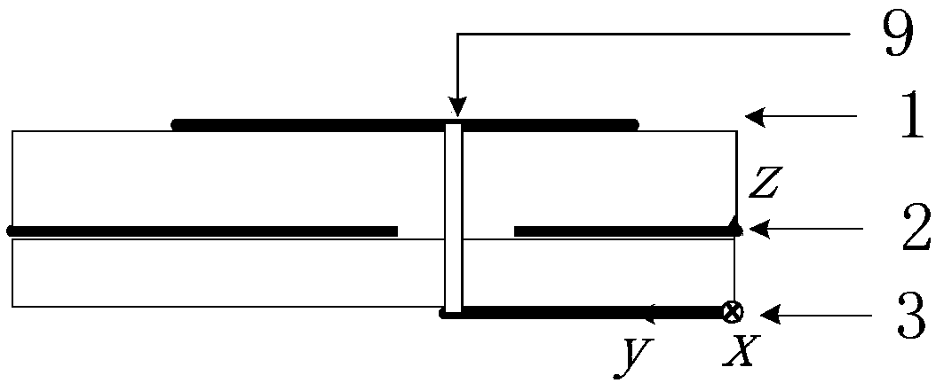
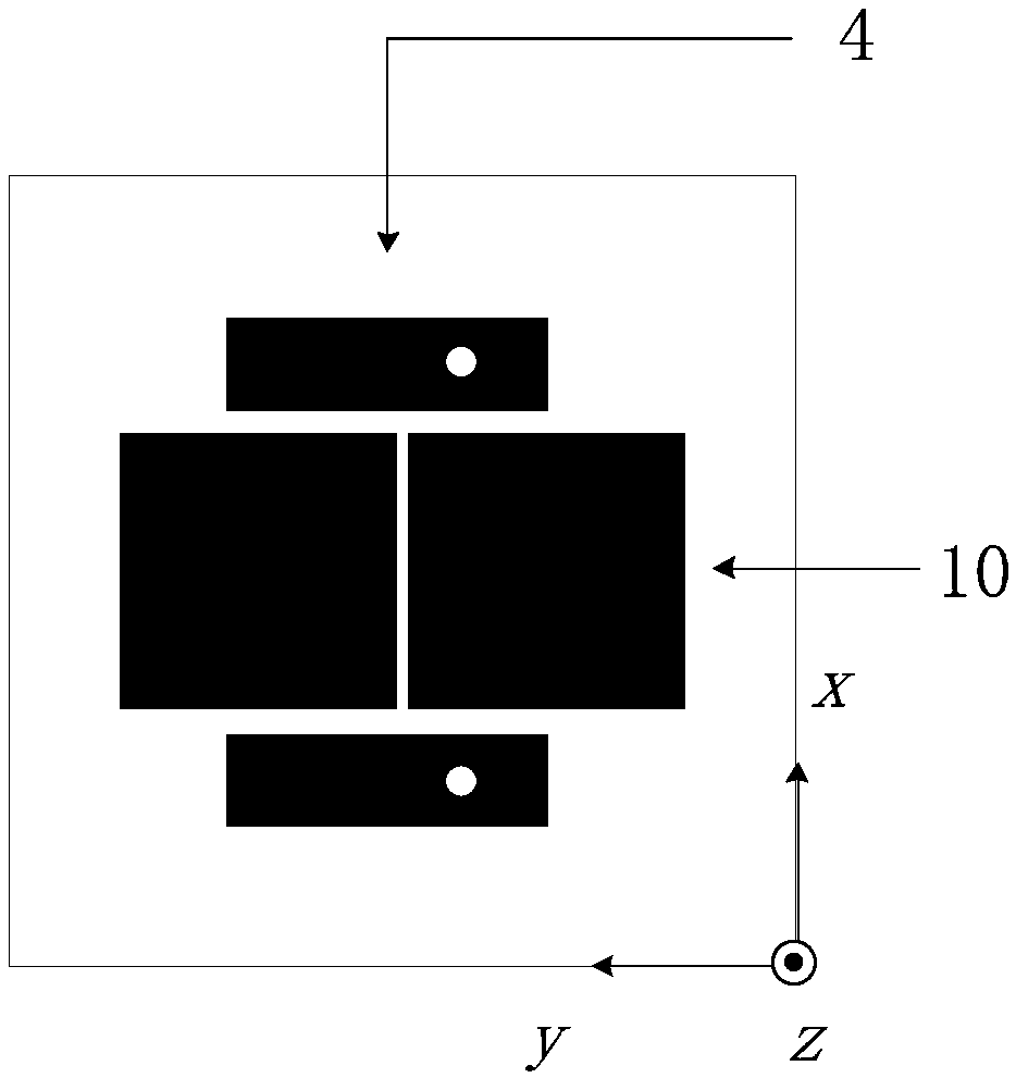
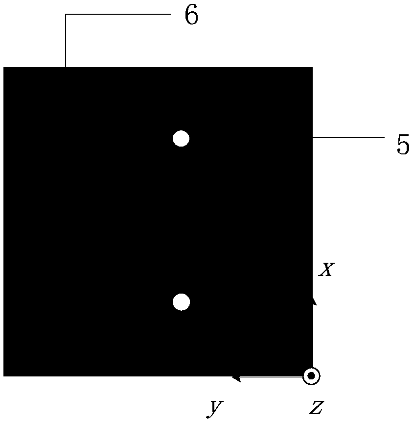
The invention discloses a millimeter-wave low-profile broadband antenna, comprising the following three-layer structures arranged in order from top to bottom: a first layer structure comprising a metal patch structure and two metal strip resonators, the metal patch structure being positioned between the two metal strip resonators; and a second layer structure comprising a metal strip resonator anda metal strip resonator. The second layer is a large metal formation with a pair of circular cracks; A third layer structure including a feeding structure connected to the two metal strip resonatorsthrough a pair of metal vias through which the pair of circular slots are pierced. The invention solves the problem that the traditional design technology requires high profile height, and realizes the wideband coverage performance of the antenna on the basis of low profile. Moreover, the metal patch structure and the two metal strip resonators are arranged in the same layer, and the single layerstructure is adopted, that is, only one layer of dielectric substrate is needed above the metal ground of the antenna, which effectively reduces the design and processing cost, realizes a wide spectrum bandwidth in a low-cost manner, and has good radiation performance in the frequency band.

Description

Technical field [0001] The present invention relates to the field of communication, in particular to a millimeter wave low-profile broadband antenna. Background technique [0002] The fifth-generation mobile communication technology is developing rapidly in the direction of high frequency, miniaturization, low cost and high performance. By taking advantage of the bandwidth advantages of millimeter wave frequency bands (for example, 28GHz, 39GHz, and 60GHz), the data transmission rate can be increased by tens of times compared with the fourth generation (from 100Mb / s to tens of Gb / s). At the same time, due to the high consumption orientation of various terminal devices, they are pursuing lightness and thinness, and in the fierce competition environment, they must give full consideration to cost and performance. In this context, a low-profile broadband antenna is designed in a low-cost manner. For example, in the 28GHz frequency band, the profile height is 0.06λ 0 And below (under...

Claims


Application Information

Patent Timeline
IPC IPC(8): H01Q1/38H01Q1/48H01Q1/50
CPCH01Q1/38H01Q1/48H01Q1/50
Inventor 施金杨汶汶杨实
Owner NOVACO MICROELECTRONICS TECH LTD
Why Eureka
Try Eureka