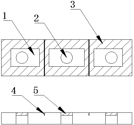
Design and manufacturing method of a ceramic wall structure based on to-shaped end seals
A manufacturing method and end-sealing technology, which are used in the manufacture of semiconductor/solid-state devices, semiconductor/solid-state device components, and semiconductor devices, etc., can solve the problem of low air-tightness of the tube and shell, micro-cracks in ceramic walls, and easy deformation of end-sealing holes, etc. problems, to achieve the effect of improving pressure resistance and impact resistance, facilitating mass production and low production cost
- Summary
- Abstract
- Description
- Claims
- Application Information
AI Technical Summary
Problems solved by technology
Method used
Image
Examples
specific Embodiment 1
[0044] A design based on a TO-type end-sealed shell-and-tube ceramic wall structure, using 98wt% alumina raw ceramics, a closed entity with a metallized connecting rib pattern width of 0.8mm, and a design of end-seal hole diameter of 1.35mm. The design is 3.7mm, and the overall dimension is designed to be 12.7mm in length and 2.6mm in width.
[0045] A method for manufacturing ceramic wall structures based on TO-type end-sealed tubular shells includes the following manufacturing steps:
[0046] 1) Make a screen with a photosensitive film thickness of 10 μm and an opening ratio of 40%, and use a multi-layer ceramic alumina printing process to control the metallization paste to a thickness of 10 μm to realize the production of metallized rib graphics.
[0047] 2) Use an ultraviolet or fiber laser with an output power of 10W and a spot diameter of 0.1mm to process a 1.4mm-diameter end-sealed hole on an alumina green ceramic sheet. The ultraviolet laser processing parameters pulse...
specific Embodiment 2
[0051] A design based on a TO-type end-sealed shell-like ceramic wall structure uses 95wt% alumina raw ceramics, and the width of the metallized connecting rib is designed to be a closed entity of 0.9mm. The diameter of the end-sealed hole is designed to be 1.5mm, and the hole pitch is designed is 3.81mm, and the overall dimension is designed to be 13mm in length and 3mm in width.
[0052] A method for manufacturing ceramic wall structures based on TO-type end-sealed tubular shells includes the following manufacturing steps:
[0053] 1) Make a screen with a photosensitive film thickness of 13 μm and an opening ratio of 65%, and use a multi-layer ceramic alumina printing process to control the metallization paste to a thickness of 15 μm to realize the production of metallized rib graphics.
[0054] 2) Use an ultraviolet laser with an output power of 10W and a spot diameter of 0.02mm to process holes with a diameter of 1.5mm on the alumina green ceramic sheet. The parameters of ...
specific Embodiment 3
[0058] A design based on a TO-type end-sealed shell-like ceramic wall structure uses 92wt% alumina raw ceramics, and the width of the metallized connecting rib is designed to be a closed entity of 1.5mm. The diameter of the end-sealed hole is designed to be 1.56mm, and the hole pitch is designed is 3.9mm, and the overall dimension is designed to be 13.2mm in length and 3.1mm in width.
[0059] A method for manufacturing ceramic wall structures based on TO-type end-sealed tubular shells includes the following manufacturing steps:
[0060] 1) Make a screen with a photosensitive film thickness of 30 μm and an aperture ratio of 70%, and use a multi-layer ceramic alumina printing process to control the metallization paste to a thickness of 50 μm to realize the production of metallized rib graphics.
[0061] 2) Use an ultraviolet laser with an output power of 20W and a spot diameter of 0.2mm to process holes with a diameter of 1.56mm on the alumina green ceramic sheet. The processin...
PUM
| Property | Measurement | Unit |
|---|---|---|
| diameter | aaaaa | aaaaa |
| thickness | aaaaa | aaaaa |
| thickness | aaaaa | aaaaa |
Abstract
Description
Claims
Application Information
 - R&D
- Intellectual Property
- Life Sciences
- Materials
- Tech Scout
- Unparalleled Data Quality
- Higher Quality Content
- 60% Fewer Hallucinations
Browse by: Latest US Patents, China's latest patents, Technical Efficacy Thesaurus, Application Domain, Technology Topic, Popular Technical Reports.
© 2025 PatSnap. All rights reserved.Legal|Privacy policy|Modern Slavery Act Transparency Statement|Sitemap|About US| Contact US: help@patsnap.com

