OLED display panel and encapsulation method thereof

A display panel and encapsulation layer technology, which is applied in the manufacture of electrical components, electrical solid devices, semiconductor/solid devices, etc., can solve the problem of water vapor/oxygen intrusion into devices, and achieve enhanced water vapor/oxygen entry into OLED display panels, saving costs, The effect of increasing the border width

Inactive Publication Date: 2018-12-07
WUHAN CHINA STAR OPTOELECTRONICS SEMICON DISPLAY TECH CO LTD
View PDF5 Cites 5 Cited by
  • Summary
  • Abstract
  • Description
  • Claims
  • Application Information

AI Technical Summary

Problems solved by technology

At present, cover plate packaging and thin film packaging are used in the market, but in certain environments such as high temperature and high humidity, or in the state of curved surfaces, there will still be water vapor / oxygen intrusion into the device. As the requirements for OLED display devices become more and more How to increase its water vapor / oxygen performance and increase its service life has become the focus of attention

Method used


Image

  • OLED display panel and encapsulation method thereof
  • OLED display panel and encapsulation method thereof
  • OLED display panel and encapsulation method thereof

Examples


Embodiment 2

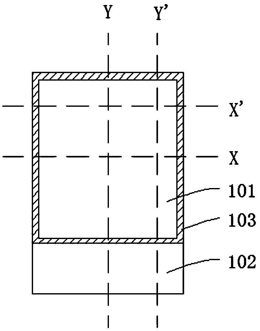
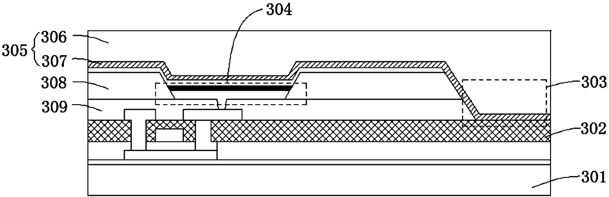
[0044] In the second embodiment, the first layer on the inner surface of the encapsulation layer 305 is an inorganic layer, and the space between the reserved area 303 and the encapsulation layer 305 is reserved in the manufacture of each film layer and structure included in the thin film transistor layer. The first inorganic layer 307 is in contact, that is, when the flat layer 309, the pixel defining layer 308 and other organic material film layers are produced, the reserved area 303 is vacant or has a hole, and when the package is produced, In this embodiment, the first inorganic layer 307 of the encapsulation layer 305 is in contact with the second inorganic material film layer in the thin film transistor layer in the reserved area 303 to form the enhanced encapsulation enclosing circle of inorganic materials. .

[0045] Such as Figure 4A As shown, it is a schematic cross-sectional view of an edge part of an OLED display panel provided by Embodiment 3 of the present inve...


PUM


Abstract

The present invention provides an OLED display panel and an encapsulation method thereof. The OLED display panel includes a substrate, a thin film transistor layer formed on the substrate, an OLED light emitting layer prepared on the thin film transistor layer, and an encapsulation layer prepared on the OLED light emitting layer, wherein the OLED light emitting layer includes an OLED light emitting device, and the encapsulation layer includes a plurality of inorganic layers and organic layers which are alternately disposed, wherein at least one of the inorganic layers in the encapsulation layer contacts at least one inorganic material film layer in the OLED light emitting layer or the thin film transistor layer through a reserved region, so that an enhancement encapsulation enclosing ringat least surrounding the OLED light emitting device can be formed so as to encapsulate the OLED display panel.

Description

technical field [0001] The invention relates to the technical field of display manufacturing, in particular to an OLED display panel and a packaging method thereof. Background technique [0002] An organic light emitting display generally includes an organic light emitting material having a first electrode, a second electrode, and an intermediate layer between the first electrode and the second electrode. Organic light-emitting displays feature wide viewing angles, high contrast, and fast response. Research has recently been conducted on making thinner display devices. Encapsulation is required in the manufacture of OLED displays, and the function of encapsulation is to prevent external water vapor / oxygen from entering the OLED display and damaging its display life. At present, cover plate packaging and thin film packaging are used in the market, but in certain environments such as high temperature and high humidity, or in the state of curved surfaces, there will still be ...

Claims


Application Information

Patent Timeline
Patent Type & Authority Applications(China)
IPC IPC(8): H01L51/52H01L27/32
CPCH10K59/12H10K50/844
Inventor 李雪云唐岳军
Owner WUHAN CHINA STAR OPTOELECTRONICS SEMICON DISPLAY TECH CO LTD
Why Eureka
Try Eureka