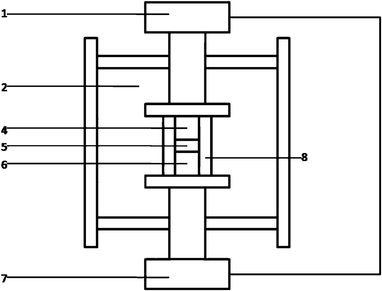
Hot-press sintering device, block thermoelectric materials of micro-nano porous structure and manufacturing method thereof
A technology of hot pressing sintering and thermoelectric materials, which is applied to the preparation of bulk thermoelectric materials and the field of hot pressing sintering devices, and can solve the problems of complex operation steps and inability to be widely used
- Summary
- Abstract
- Description
- Claims
- Application Information
AI Technical Summary
Problems solved by technology
Method used
Image
Examples
Embodiment 1
[0081] This embodiment is used to illustrate Zintl phase thermoelectric material Mg 3.175 mn 0.025 Sb 1.98 Bi 0.5 Te 0.02 and its preparation.
[0082] Firstly, the simple substance particles of each element are ball milled for 12 hours according to the stoichiometry to form a powder with a particle size of 200 nanometers to 10 microns. The conventional spark plasma sintering method sinters the powder into a dense block (this process is a sintering), and the sintering conditions are as follows: vacuum degree 5Pa, pressure 50MPa, heating rate 50℃ / min, sintering temperature 600℃, holding time 5 minute.
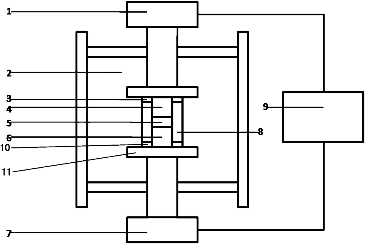
[0083] Then ball mill the primary sintered bulk material for 4 hours to form a raw material powder with a particle size of 200 nanometers to 10 microns. figure 2 Secondary sintering was performed in the device shown to obtain samples with multiscale micro-nanoporous structures. In the secondary sintering, the vacuum degree is 5Pa, the pressure is 50MPa, the heating rate ...
Embodiment 2
[0088] This embodiment is used to illustrate the Half-Heusler alloy thermoelectric material Hf 0.25 Zr 0.75 NiSn 0.99 Sb 0.01 and its preparation.
[0089] First, according to the stoichiometric ratio, the simple substances of each element are arc-melted into ingots, and then ball milled for 12 hours to form a powder with a particle size of 200-600 nanometers. figure 2 Spark plasma sintering is carried out in the device shown, the vacuum degree is 5Pa, the pressure is 60MPa, the heating rate is 40°C / min, the sintering temperature is 900°C, and the holding time is 20 minutes. Samples with scale micro-nanoporous (porous) structures.
[0090] Figure 5 and Figure 6 Representative SEM images of samples of Example 2 at different magnifications are shown. SEM results show that the sample of Example 2 has a multi-scale micro-nano pore (porous) structure. The compactness of the sample of Example 2 is 93%.
[0091] In addition, the FDS-4000 spark plasma sintering furnace joi...
Embodiment 3
[0094] This example is used to illustrate Bi 2 Te 3 Base material Bi 0.5 Sb 1.5 Te 3 and its preparation.
[0095] Firstly, ball mill the elemental particles of each element for 9 hours according to stoichiometry to form a powder with a particle size of 100-300 nanometers. figure 2 Spark plasma sintering is carried out in the device shown, the vacuum degree is 5Pa, the pressure is 50MPa, the heating rate is 70°C / min, the sintering temperature is 450°C, and the holding time is 5 minutes. Samples with scale micro-nanoporous (porous) structures.
[0096] Figure 7 and Figure 8 Representative SEM images of samples of Example 3 at different magnifications are shown. SEM results show that the sample of Example 3 has a multi-scale micro-nano pore (porous) structure. The compactness of the sample of Example 3 is 81%.
[0097] In addition, Bi 0.5 Sb 1.5 Te 3 dense material as a reference sample. Specifically, firstly, according to the stoichiometry, the simple substance...
PUM
| Property | Measurement | Unit |
|---|---|---|
| Particle size | aaaaa | aaaaa |
| Thermal conductivity | aaaaa | aaaaa |
Abstract
Description
Claims
Application Information
 - R&D
- Intellectual Property
- Life Sciences
- Materials
- Tech Scout
- Unparalleled Data Quality
- Higher Quality Content
- 60% Fewer Hallucinations
Browse by: Latest US Patents, China's latest patents, Technical Efficacy Thesaurus, Application Domain, Technology Topic, Popular Technical Reports.
© 2025 PatSnap. All rights reserved.Legal|Privacy policy|Modern Slavery Act Transparency Statement|Sitemap|About US| Contact US: help@patsnap.com


