Piezoelectric device, liquid discharging head, and liquid discharging apparatus

一种压电器件、压电元件的技术,应用在压电/电致伸缩/磁致伸缩器件、压电器件的或电致伸缩器件的零部件、电气元件等方向,能够解决龟裂、振动板出现裂纹、妨碍振动板位移等问题

Active Publication Date: 2018-12-04
SEIKO EPSON CORP
View PDF12 Cites 1 Cited by
  • Summary
  • Abstract
  • Description
  • Claims
  • Application Information

AI Technical Summary

Problems solved by technology

[0003] However, since the vibration plate of Patent Document 1 is composed of a single-layer silicon substrate, depending on the crystal plane of the silicon substrate used, the Young's modulus may vary depending on the direction within the crystal plane.
When the vibrating plate is formed of such a silicon base material, for example, since the crystal orientation with a large Young's modulus is less likely to warp than the crystal orientation with a small Young's modulus, it may hinder the overall Displacement of the vibrating plate
On the other hand, since the vibrating plate tends to bend in the crystal orientation with a small Young's modulus, cracks (cracks) tend to occur on the vibrating plate or the piezoelectric element when it is flexed excessively
However, since the crystal orientation is not taken into consideration in the shape of the pressure chamber or the piezoelectric element in Patent Document 1, if there is an orientation with a different Young's modulus around the vibration plate, it may hinder the vibration of the vibration plate as a whole. displacement, or prone to cracks

Method used


Image

  • Piezoelectric device, liquid discharging head, and liquid discharging apparatus
  • Piezoelectric device, liquid discharging head, and liquid discharging apparatus
  • Piezoelectric device, liquid discharging head, and liquid discharging apparatus

Examples


no. 1 approach

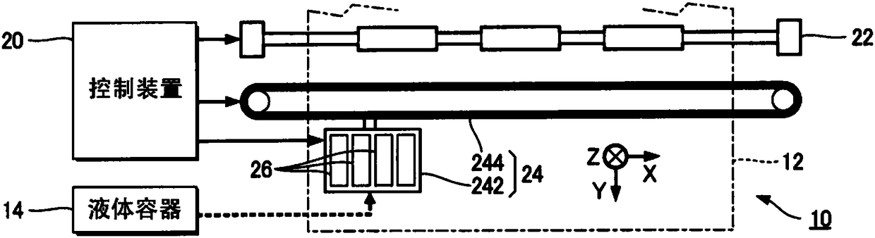
[0034] figure 1 It is a configuration diagram illustrating an example of the liquid ejection device 10 according to the first embodiment of the present invention. The liquid ejection device 10 of the first embodiment is an inkjet printing device that ejects ink as an example of a liquid onto a medium 12 . The medium 12 is typically printing paper, but any printing target such as a resin film or cloth can also be used as the medium 12 . like figure 1 As shown, a liquid container 14 for storing ink is fixed in the liquid ejection device 10 . As the liquid container 14 , for example, an ink cartridge detachable from the liquid ejection device 10 , a pouch-shaped ink pack formed of a flexible film, or an ink tank capable of replenishing ink can be used. A plurality of inks of different colors are stored in the liquid container 14 .

[0035] like figure 1 As shown, the liquid ejection device 10 includes a control device 20 , a transport mechanism 22 , a moving mechanism 24 , a...

no. 2 approach

[0087] A second embodiment of the present invention will be described. In each of the embodiments exemplified below, the symbols used in the description of the first embodiment are used for the elements having the same functions or functions as those of the first embodiment, and detailed descriptions thereof are appropriately omitted. While the first embodiment exemplifies the case where the vibration plate 36 is formed from a single crystal silicon substrate whose crystal plane is the (100) plane, the second embodiment exemplifies the case where the crystal plane is the (110) plane A case where the vibration plate 36 is formed of a single crystal silicon substrate (the crystal plane orientation perpendicular to the crystal plane is [110]).

[0088] Figure 10 It is a graph showing an example of the anisotropy of Young's modulus in the (110) plane of a single crystal silicon base material whose crystal plane is the (110) plane. exist Figure 10 middle, Figure 10 is a pola...

no. 3 approach

[0107] A third embodiment of the present invention will be described. While in the first and second embodiments, the case where the outer edge 37B of the piezoelectric element 37 has a shape similar to the shape of the inner edge 37A was exemplified, in the third embodiment, the piezoelectric element 37 is exemplified The shape of the outer edge 37B is not a shape similar to the shape of the inner edge 37A.

[0108] The width T of the piezoelectric element 37 is the width between the inner edge 37A and the outer edge 37B. For example, if Figure 4 As shown, the width T of the piezoelectric element 37 can be divided into the width Ta of the portion overlapping the above-mentioned pressure chamber C in plan view and the width Tb of the portion overlapping the side wall 344 of the pressure chamber C in plan view. . The width Ta of the piezoelectric element 37 is the width of the inner peripheral portion 372a, and the width Tb is the width of the outer peripheral portion 372b. ...


PUM


Abstract

According to an aspect of the invention, the generation of cracks can be inhibited and the displacement efficiency can be improved. A piezoelectric device including a pressure chamber, a piezoelectricelement, and a diaphragm disposed between the pressure chamber and the piezoelectric element. The diaphragm has a crystal plane {100} of a single crystal silicon base. The piezoelectric element is disposed on the diaphragm so as to overlap an inner periphery of the pressure chamber in plan view, and has an inner edge on a center side of the pressure chamber with the inner periphery of the pressure chamber being sandwiched within the piezoelectric element in plan view. A shape of the inner edge of the piezoelectric element is such that in the smallest first rectangle, which includes the inneredge in plan view, the inner edge is on the inside of each of sides at a middle portion of each of the sides of the first rectangle. A shape of the inner periphery of the pressure chamber is such thatin the smallest second rectangle, which includes the inner periphery in plan view, the inner periphery is on the inside of each of sides at a middle portion of each of the sides of the second rectangle. A direction of one side out of the first rectangle and the second rectangle lies along a crystal orientation <010> in the crystal plane.

Description

technical field [0001] The present invention relates to a technology for generating pressure fluctuations by piezoelectric devices. Background technique [0002] Conventionally, there has been proposed a liquid ejection head in which liquid such as ink supplied to the pressure chamber is ejected from nozzles by varying the pressure of the pressure chamber using a piezoelectric device. For example, Patent Document 1 discloses that a vibrating plate (diaphragm) having a wall surface (upper surface) constituting the pressure chamber (increasing chamber) and a piezoelectric device vibrating the vibrating plate are provided for each pressure chamber. Components of piezoelectric device technology. The piezoelectric element is arranged on the peripheral portion of the circular pressure chamber, and by using the piezoelectric element, the vibration region overlapping with the pressure chamber in plan view in the vibration plate made of a single-layer silicon base material is reduce...

Claims


Application Information

Patent Timeline
Patent Type & Authority Applications(China)
IPC IPC(8): B41J2/14
CPCB41J2/14233H10N30/10513H10N30/2047B41J2/14274H10N30/80
Inventor 田村博明山崎清夏
Owner SEIKO EPSON CORP
Why Eureka
Try Eureka