Manufacturing method of array substrate, array substrate and display device

The technology of an array substrate and a manufacturing method, which is applied in the field of array substrates and display devices, can solve problems such as complex manufacturing process steps of array substrates, achieve good electrical connection performance, and simplify the manufacturing process

Active Publication Date: 2020-07-03
BOE TECH GRP CO LTD
View PDF6 Cites 0 Cited by
  • Summary
  • Abstract
  • Description
  • Claims
  • Application Information

AI Technical Summary

Problems solved by technology

However, in order to ensure a good electrical connection between the light-shielding layer and the source / drain electrode layer of the thin film transistor, the via holes made in the interlayer dielectric layer and the buffer layer mostly adopt a nested hole structure, which requires two patterning process, that is, two different masks are used to make the set of holes, resulting in more complicated manufacturing process steps of the array substrate

Method used


Image

  • Manufacturing method of array substrate, array substrate and display device
  • Manufacturing method of array substrate, array substrate and display device
  • Manufacturing method of array substrate, array substrate and display device

Examples


Embodiment Construction

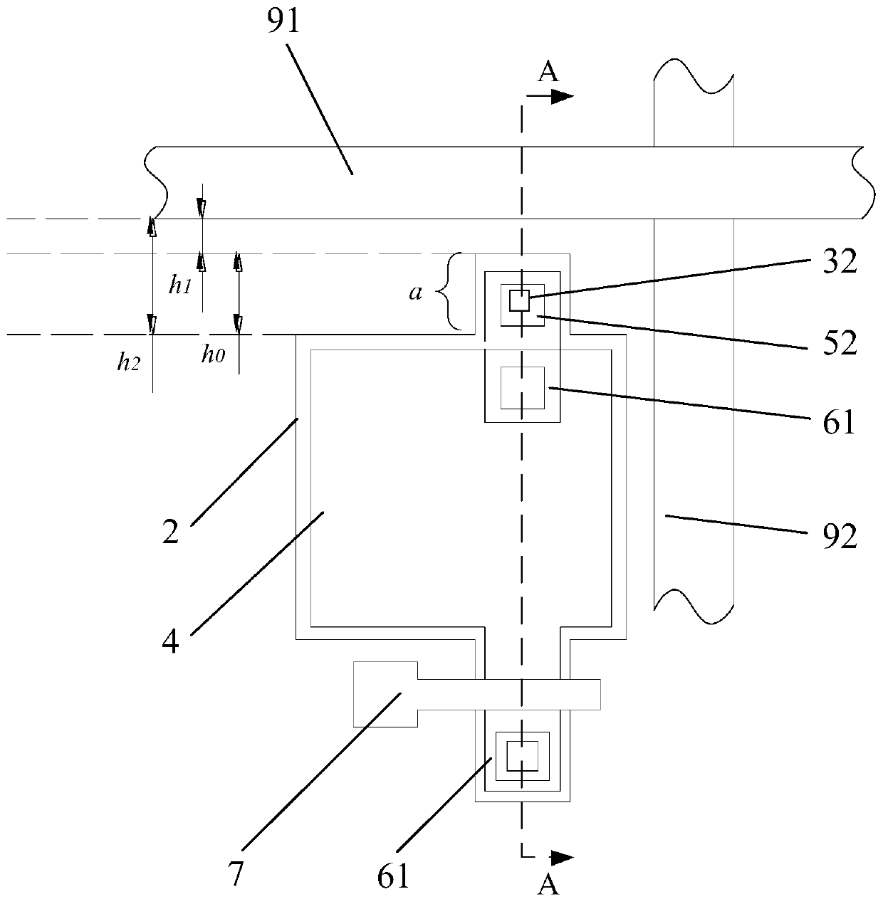
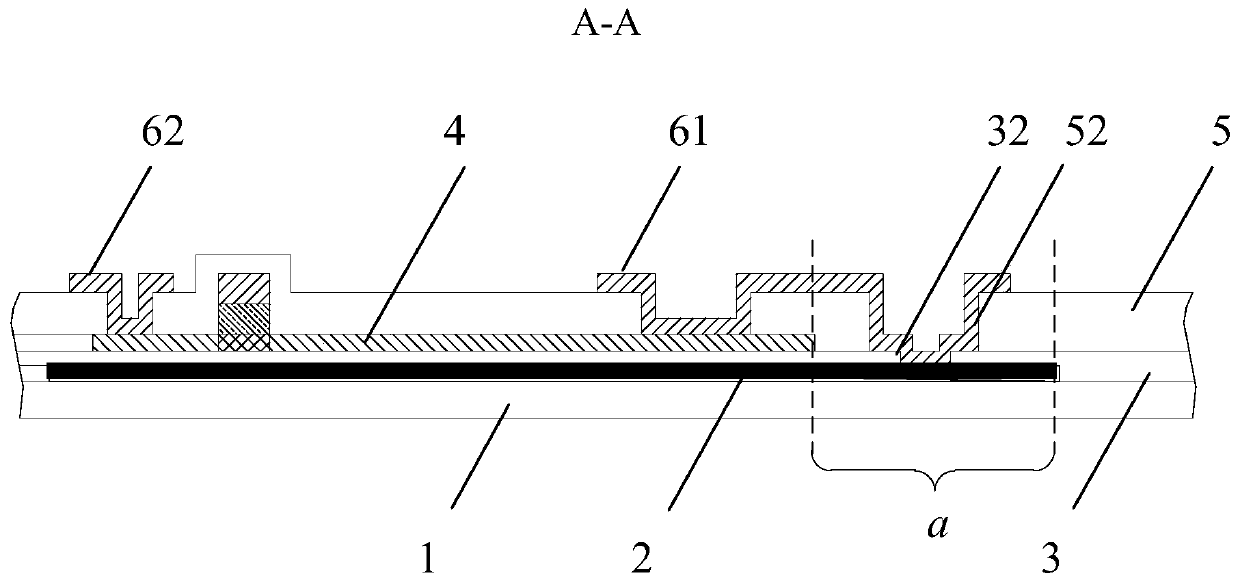
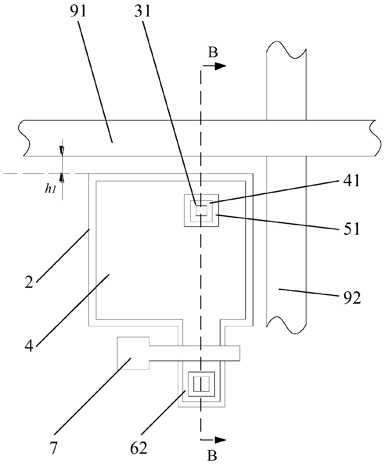
[0043] In order to make the above objects, features and advantages of the embodiments of the present disclosure more obvious and understandable, the technical solutions in the embodiments of the present disclosure will be clearly and completely described below in conjunction with the accompanying drawings. Apparently, the described embodiments are only some of the embodiments of the present disclosure, not all of them. Based on the embodiments in the present disclosure, all other embodiments obtained by persons of ordinary skill in the art without creative efforts fall within the protection scope of the present disclosure.

[0044] It can be understood that the one-time patterning process involved in the related technologies and the embodiments of the present disclosure generally refers to the process of making a mask on the surface of the material to be etched and using the mask to pattern the material to be etched ; That is to say, if a mask is made once, it is considered th...


PUM


Abstract

The disclosure discloses a manufacturing method of an array substrate, an array substrate and a display device, relates to the field of display technology, and is used to simplify the manufacturing process of the array substrate. The manufacturing method of the array substrate includes: sequentially forming a light-shielding layer and a buffer layer on the base substrate; forming an active layer on the buffer layer, and forming a first via hole in the active layer; forming an interlayer on the active layer dielectric layer; through a patterning process, a second via hole is formed in the position corresponding to the first via hole in the interlayer dielectric layer, and a third via hole is formed in the position corresponding to the first via hole in the buffer layer; in the interlayer dielectric layer A source / drain electrode layer is formed on it, so that the source / drain electrode layer is electrically connected to the light-shielding layer through the second via hole, the first via hole and the third via hole in sequence. The manufacturing method of the array substrate, the array substrate and the display device provided by the present disclosure are used for the array substrate manufactured by using top-gate thin film transistors.

Description

technical field [0001] The present disclosure relates to the field of display technology, and in particular, to a method for manufacturing an array substrate, the array substrate and a display device. Background technique [0002] In the related art, when a top-gate (Top Gate) thin-film transistor is used to make an array substrate, the structure of the top-gate thin-film transistor usually includes: an active layer (Active) and a gate insulating layer arranged on one side of the substrate in sequence. (GI), gate (GT), interlayer dielectric layer (ILD) and source / drain electrode layer (S / D). [0003] In order to prevent external ambient light from directly striking the active layer and adversely affecting the working characteristics of the thin film transistor, a light shielding layer is usually provided between the active layer and the base substrate. A buffer layer (Buffer) is usually disposed between the light shielding layer and the active layer. [0004] The above-men...

Claims


Application Information

Patent Timeline
Patent Type & Authority Patents(China)
IPC IPC(8): H01L27/12
CPCH01L27/1222H01L27/1237H01L27/1248H01L29/78633H01L29/41733H10K19/10H01L27/1225H01L27/124H01L27/1288H01L29/458H01L29/4908H01L29/78666H01L29/78675H01L29/7869H01L29/78693H10K10/84H10K10/471H10K10/472H10K10/481H10K10/488H10K59/125H10K59/126H10K59/131H10K59/1213
Inventor 宋振王国英
Owner BOE TECH GRP CO LTD
Why Eureka
Try Eureka