Shallow-groove isolation structure transverse semiconductor device arranged in staggered and interdigital way

A lateral semiconductor, shallow trench isolation technology, applied in semiconductor devices, semiconductor/solid-state device manufacturing, electrical components, etc., can solve the problems of increased device on-resistance, inability to achieve compromise, and increased flow paths, reducing Small surface electric field, reduced impact ionization rate, and uniform electric field distribution

Active Publication Date: 2018-11-13
SOUTHEAST UNIV
View PDF4 Cites 4 Cited by
  • Summary
  • Abstract
  • Description
  • Claims
  • Application Information

AI Technical Summary

Problems solved by technology

Although this process can improve the withstand voltage capability of the device, the STI structure will increase the flow path of the current from the source to the drain, resulting in an increase in the on-resistance of the device.
Therefore, when the STI structure is used in the drift region of LDMOS, a better compromise between breakdown voltage and on-resistance cannot be achieved.

Method used


Image

  • Shallow-groove isolation structure transverse semiconductor device arranged in staggered and interdigital way
  • Shallow-groove isolation structure transverse semiconductor device arranged in staggered and interdigital way
  • Shallow-groove isolation structure transverse semiconductor device arranged in staggered and interdigital way

Examples


Embodiment Construction

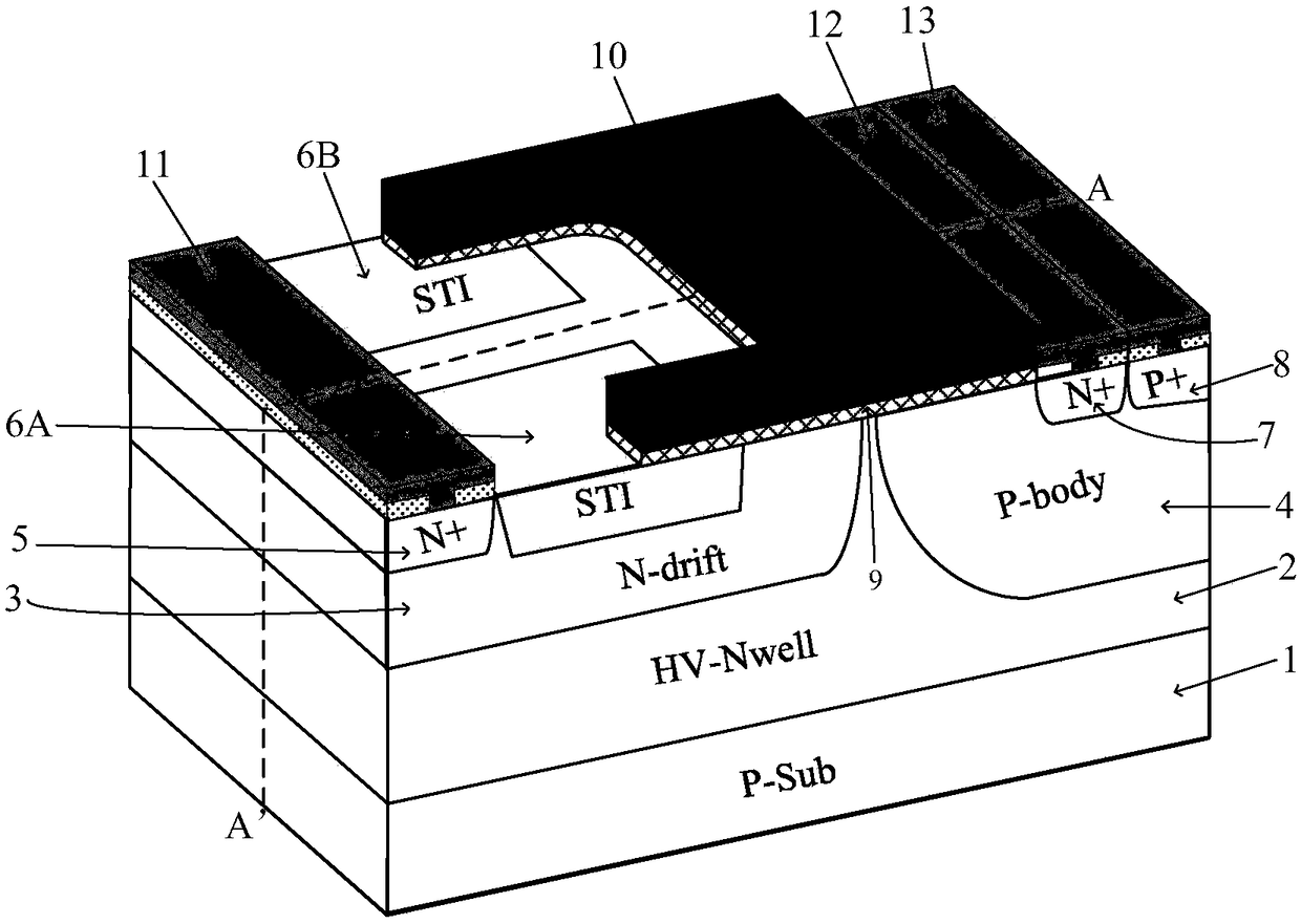
[0019] A lateral semiconductor device with an interdigitated shallow trench isolation structure, comprising: a P-type substrate 1, a high-voltage N-type region 2 is arranged above the P-type substrate 1, and a high-voltage N-type region 2 is arranged above the high-voltage N-type region 2. The N-type drift region 3 and the P-type body region 4 are provided with an N-type drain region 5, a first shallow trench isolation region 6A, a second shallow trench isolation region 6B and a third shallow trench isolation region 6C in the N-type drift region 3 In the P-type body region 4, an N-type source region 7 and a P-type region 8 are arranged, and a U-shaped gate oxide layer 9 is also arranged on the high-voltage N-type region 2, and the U-shaped opening of the gate oxide layer 9 faces the drain and both ends extend to the top of the P-type body region 4 and the top of the first shallow trench isolation region 6A and the third shallow trench isolation region 6C, and a polysilicon gate...


PUM


Abstract

A shallow-groove isolation structure transverse semiconductor device arranged in a staggered and interdigital way comprises a P-type substrate, wherein a high-voltage N-type region is arranged on theP-type substrate, an N-type drift region and a P-type body region are arranged on the high-voltage N-type region, an N-type drain region and three shallow-groove isolation regions are arranged in theN-type drift region, an N-type source region and a P-type region are arranged in the P-type body region, a U-shaped gate oxide layer is further arranged on the high-voltage N-type region, a U-shaped opening of the gate oxide layer faces a drain end, two ends of the gate oxide layer respectively extend to a part above the P-type body region and a part above the shallow-groove isolation regions, a poly-silicon gate field plate is arranged on the gate oxide layer, drain metal contact, source metal contact and body region metal contact are respectively arranged on upper surfaces of the N-type drain region, the N-type source region and the P-type region, and the shallow-groove isolation structure transverse semiconductor device is characterized in that the shallow-groove isolation regions are arranged in the drift region in the staggered and interdigital way. By the structure, relatively low conduction resistance can be obtained on the basis that the breakdown voltage is not changed.

Description

technical field [0001] The invention relates to the field of power semiconductor devices, and relates to a lateral semiconductor device with an interdigitated shallow trench isolation structure. Background technique [0002] Lateral Double-Diffused MOSFET (LDMOS) has the advantages of high breakdown voltage, high input impedance and easy integration with other devices, and is widely used in high-voltage integrated circuits and power integrated circuits . Compared with traditional MOSFET devices, LDMOS devices have a low-doped drift region. When a high voltage is applied between the drain and source, the drift region is completely depleted, so it can withstand a higher voltage. [0003] In the design of the LDMOS device structure, shallow trench isolation technology (Shallow Trench Isolation, STI) is often used in the drift region to improve the withstand voltage capability of the device. For LDMOS devices with STI structure, STI can bear most of the electric field in the d...

Claims


Application Information

Patent Timeline
Patent Type & Authority Applications(China)
IPC IPC(8): H01L29/78H01L29/06H01L21/336
CPCH01L29/0653H01L29/66681H01L29/7816H01L29/4238H01L29/0692
Inventor 刘斯扬陈虹廷叶然吴海波孙伟锋陆生礼时龙兴
Owner SOUTHEAST UNIV
Why Eureka
Try Eureka