Image sensor and forming method thereof
An image sensor and filter technology, applied in the direction of electric solid devices, semiconductor devices, electrical components, etc., can solve the problems of reducing the color saturation of the output image, poor image effect, etc., to improve the color saturation and increase the absorption effect. Effect
- Summary
- Abstract
- Description
- Claims
- Application Information
AI Technical Summary
Problems solved by technology
Method used
Image

Examples
Embodiment Construction
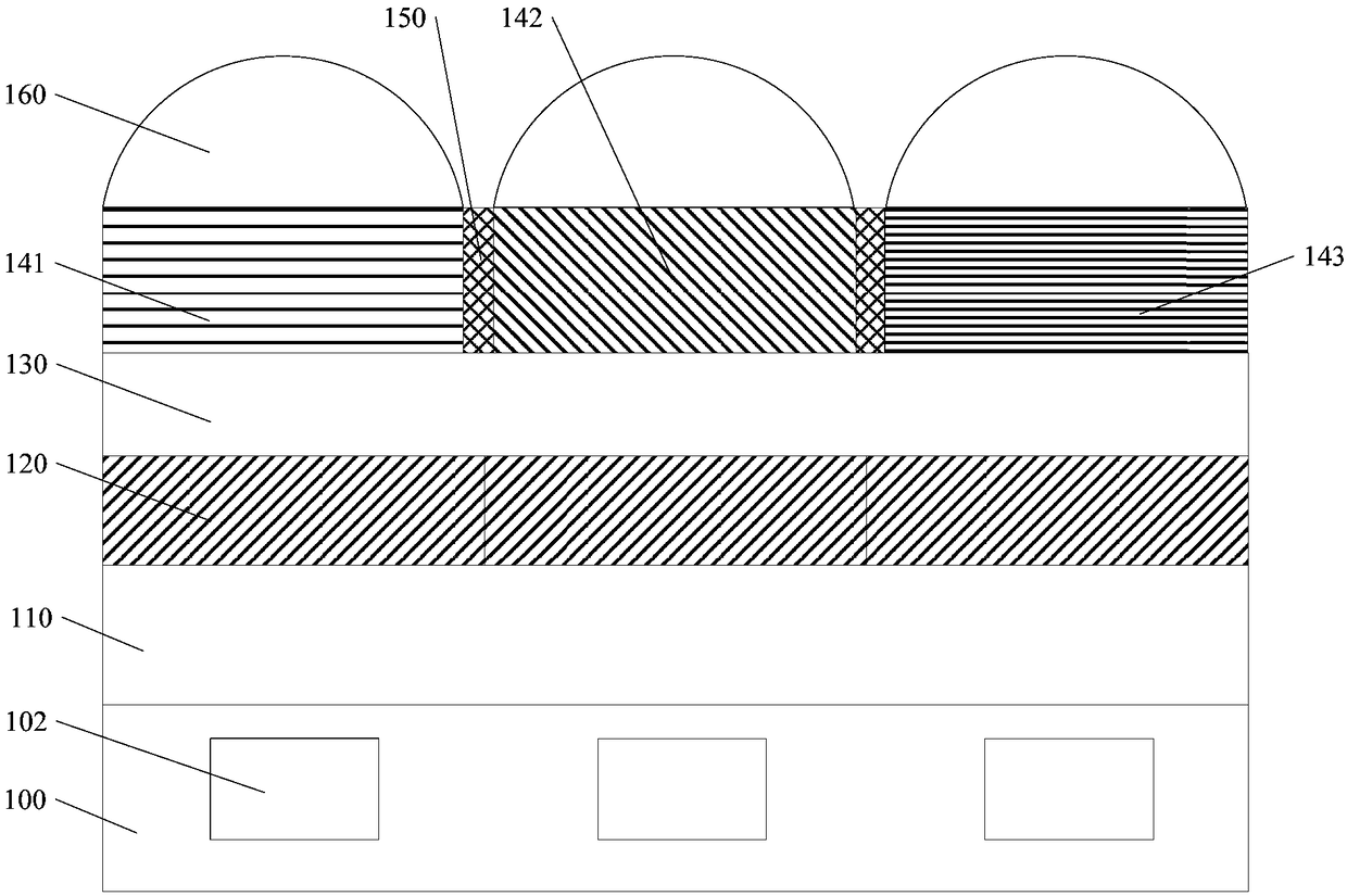
[0031] In the prior art, by setting an anti-reflection film, the pixel device in the semiconductor substrate can obtain more incident light passing through the filter matrix, and then absorb the incident photons passing through each filter through the photodiode And form a photocurrent.
[0032] However, in the prior art, the anti-reflection film has a uniform thickness and is only suitable for green light, and has a large reflectivity for red and blue light, resulting in reduced color saturation of the output image, especially in low-light conditions , the image quality is even worse.
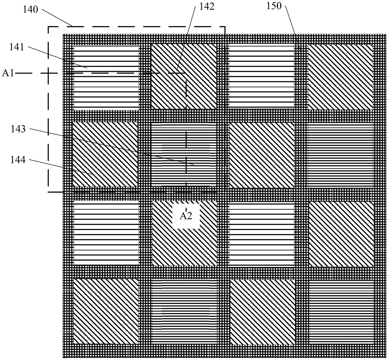
[0033] combined reference figure 1 and figure 2 , figure 1 is a top view of an image sensor in the prior art, figure 2 Yes figure 1 Sectional view along cutting line A1-A2.
[0034] The image sensor may include a semiconductor substrate 100, a pixel device 102, an anti-reflection film 120, and a filter matrix. Wherein, the pixel device 102 may be located in the semiconductor substrate...
PUM
 Abstract
Description
Claims
Application Information
 - R&D
- Intellectual Property
- Life Sciences
- Materials
- Tech Scout
- Unparalleled Data Quality
- Higher Quality Content
- 60% Fewer Hallucinations
Browse by: Latest US Patents, China's latest patents, Technical Efficacy Thesaurus, Application Domain, Technology Topic, Popular Technical Reports.
© 2025 PatSnap. All rights reserved.Legal|Privacy policy|Modern Slavery Act Transparency Statement|Sitemap|About US| Contact US: help@patsnap.com