
CIS detecting device for circuit boards

A detection device and circuit board technology, which is applied in the direction of measurement device, use feedback control, optical test flaws/defects, etc., can solve the problems of idle number, shortage, and poor application flexibility of cameras, so as to improve detection accuracy and simplify equipment structure , the effect of solving the problem of diffuse reflection

Pending Publication Date: 2018-11-06
佛山市坦斯盯科技有限公司
View PDF0 Cites 0 Cited by
  • Summary
  • Abstract
  • Description
  • Claims
  • Application Information

AI Technical Summary

Problems solved by technology

When inspecting multiple circuit boards at the same time, multiple area array cameras are set side by side, and each camera takes a picture of a circuit board. Therefore, it is necessary to pre-set the number of simultaneously inspected circuit boards, and then set the number of cameras. Changes, the cameras appear to be idle or the number is insufficient, and the flexibility of the equipment application is poor

Method used


Image

  • CIS detecting device for circuit boards
  • CIS detecting device for circuit boards
  • CIS detecting device for circuit boards

Examples


Embodiment Construction

[0040] The technical solutions of the present invention will be further described below in conjunction with the accompanying drawings and specific embodiments.

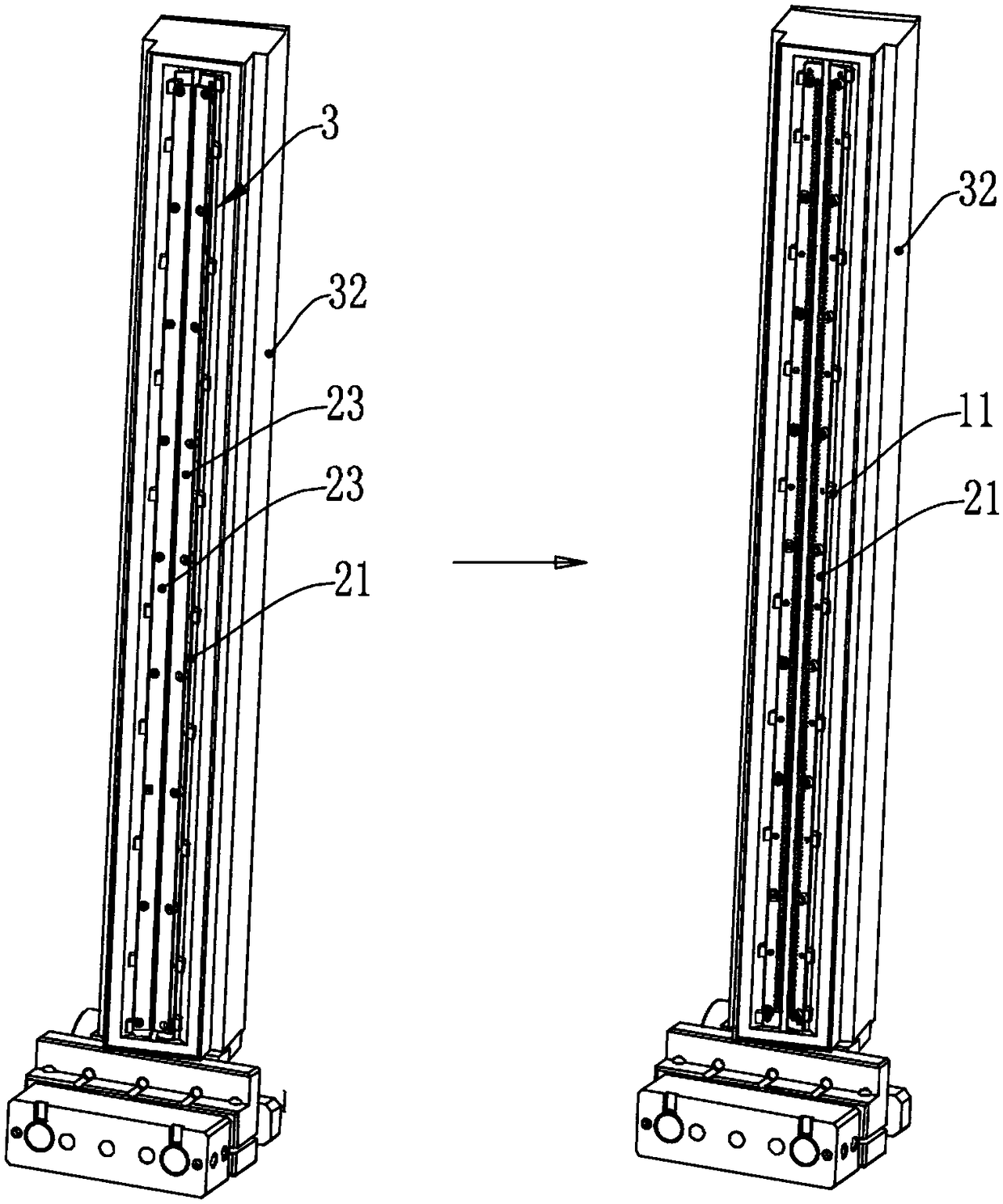
[0041] Such as figure 1 As shown, a CIS detection device for circuit boards includes a CIS line scan camera 1, a linear light source 2 and a circuit board conveying mechanism 3. Both sides of the CIS line scan camera 1 are provided with a linear light source 2, and the CIS line scan camera The optical axis of 1 and the chief ray of linear light source 2 intersect on the same straight line of the circuit board on the circuit board conveying mechanism 3;

[0042] The CIS line scan camera 1 and the linear light source 2 have the same length, the linear light source 2 is installed at the bottom of the CIS line scan camera 1 , and the CIS line scan camera 1 and the linear light source 2 straddle the circuit board conveying mechanism 3 .

[0043] During detection, the circuit board is carried by the circuit board conveying...


PUM


Abstract

The invention discloses a CIS detecting device for circuit boards. The CIS detecting device comprises CIS line array cameras, linear light sources and a circuit board conveying mechanism; the linear light sources are arranged at the two sides of the CIS line array cameras, the optical axes of the CIS line array cameras and main light of the linear light sources intersect on the same straight lineof the circuit boards on the circuit board conveying mechanism; the length of the CIS line array cameras is the same as that of the linear light sources, the linear light sources are installed at thebottoms of the CIS line array cameras, and the CIS line array cameras and the linear light sources stretch across the circuit board conveying mechanism. The CIS line array cameras can simultaneously take continuous images of a portion which is located below the cameras and is comparable to the camera in length. When the number of the circuit boards needs which need to be simultaneously detected ischanged, the number of the circuit boards can be increased or decreased by adjusting the distance between every two circuit boards, so that the number of the detected circuit boards is flexibly set within a certain range without being influenced by the size of the circuit boards. Therefore, the application flexibility of the detecting device is higher, and the equipment cost is reduced.

Description

technical field [0001] The invention relates to the technical field of circuit board detection, in particular to a CIS detection device for circuit boards. Background technique [0002] With the development of electronic technology, the functions of various electronic products are constantly upgraded, and there are higher requirements for the production and testing process of circuit boards. For example, the number of layers of circuit boards is increasing, the internal circuits are becoming denser, the line width and line spacing are smaller, and the detection accuracy is required to be high, etc. [0003] The circuit board inspection device is an advanced online inspection technology. It obtains the image information of the surface of the tested part and compares it with the image information of the qualified part, so as to detect whether the tested part is qualified. Due to the complexity of PCB boards, more and more design circuits, and more and more layers, the use of ...

Claims


Application Information

Patent Timeline
IPC IPC(8): G01N21/956G01N21/88G01N21/01G05D3/12
CPCG05D3/12G01N21/01G01N21/8806G01N21/8851G01N21/956G01N2021/0112G01N2021/95638G01N2201/06186G01N2201/0631
Inventor 门光辉
Owner 佛山市坦斯盯科技有限公司
Learn More