Semiconductor saturable absorber mirror structure with strain compensation
A saturable absorption and strain compensation technology, used in laser parts, electrical components, lasers, etc., can solve the problems of high damage threshold, increase the number of quantum wells, etc., and achieve the effect of improving life, reducing maintenance costs and reducing deformation.
- Summary
- Abstract
- Description
- Claims
- Application Information
AI Technical Summary
Problems solved by technology
Method used
Image
Examples
Embodiment Construction
[0019] The features of the present invention and other relevant features are described in further detail below through the embodiments, so as to facilitate the understanding of those skilled in the art:
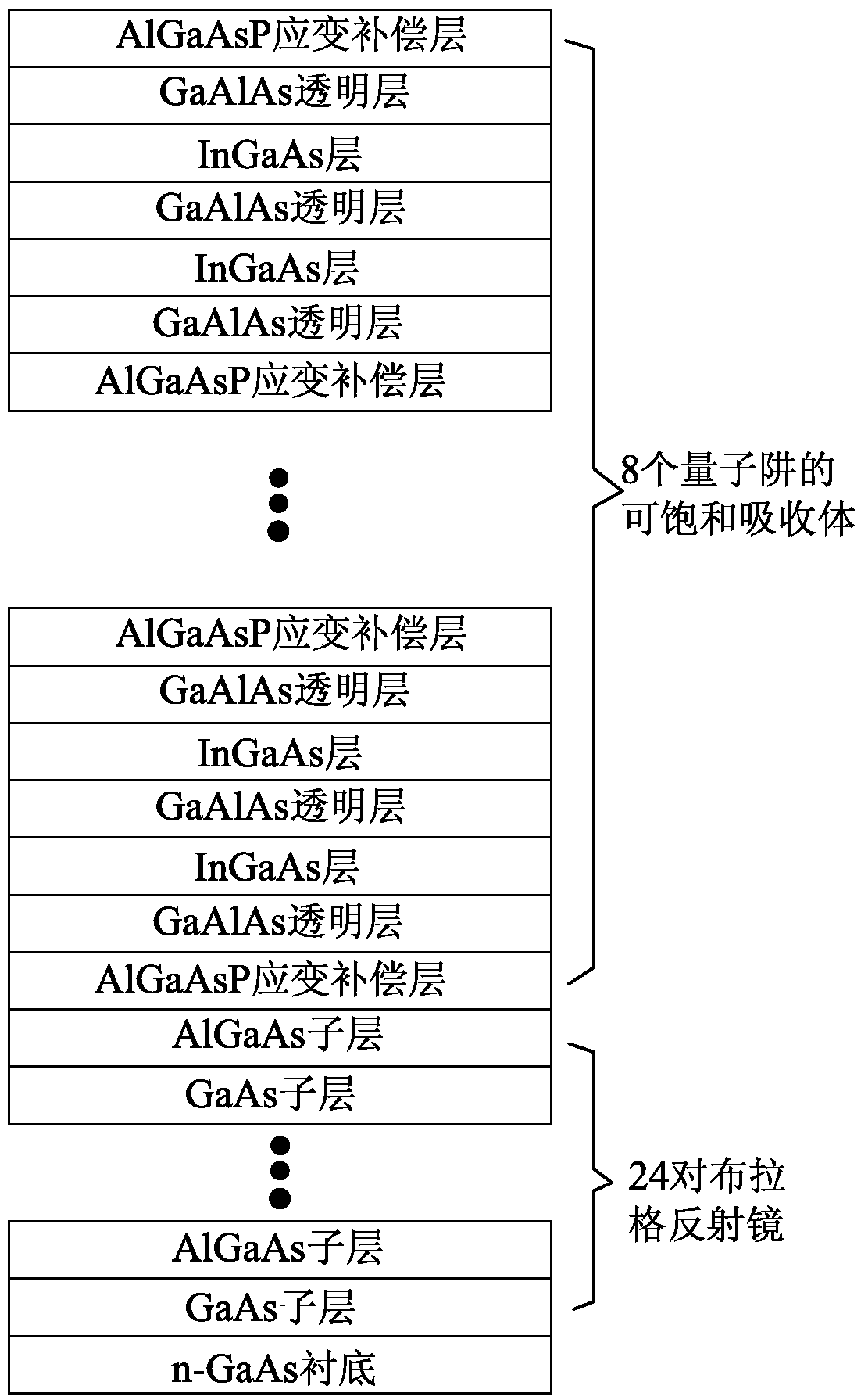
[0020] Such as figure 1 As shown, a semiconductor saturable absorber mirror structure with strain compensation is characterized in that it includes an n-GaAs substrate, and 24 pairs of Bragg mirrors and 8 quantum wells are sequentially grown on the n-GaAs substrate. A saturable absorber, wherein the thickness of each pair of Bragg mirrors is 0.25λ, λ is the design wavelength, the thickness of each quantum well is 0.5λ, and each pair of Bragg mirrors includes sequential GaAs sublayers and AlGaAs sublayers, The thickness of the GaAs sublayer ≤ the thickness of the AlGaAs sublayer, each quantum well includes a sequence of AlGaAsP strain compensation layer, GaAlAs transparent layer, InGaAs layer, GaAlAs transparent layer, InGaAs layer, GaAlAs transparent layer, AlGaAsP strain com...
PUM
 Abstract
Description
Claims
Application Information
 - R&D Engineer
- R&D Manager
- IP Professional
- Industry Leading Data Capabilities
- Powerful AI technology
- Patent DNA Extraction
Browse by: Latest US Patents, China's latest patents, Technical Efficacy Thesaurus, Application Domain, Technology Topic, Popular Technical Reports.
© 2024 PatSnap. All rights reserved.Legal|Privacy policy|Modern Slavery Act Transparency Statement|Sitemap|About US| Contact US: help@patsnap.com


