Housing, preparation method thereof and electronic device
A technology of shell and conductive layer, used in nonlinear optics, instruments, optics, etc.
- Summary
- Abstract
- Description
- Claims
- Application Information
AI Technical Summary
Problems solved by technology
Method used
Image

Examples
Embodiment Construction
[0019] The following describes in detail the embodiments of the present invention, examples of which are illustrated in the accompanying drawings. The embodiments described below with reference to the accompanying drawings are exemplary, and are intended to explain the present invention and should not be construed as limiting the present invention.
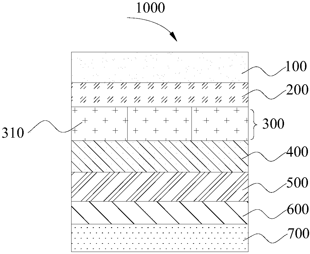
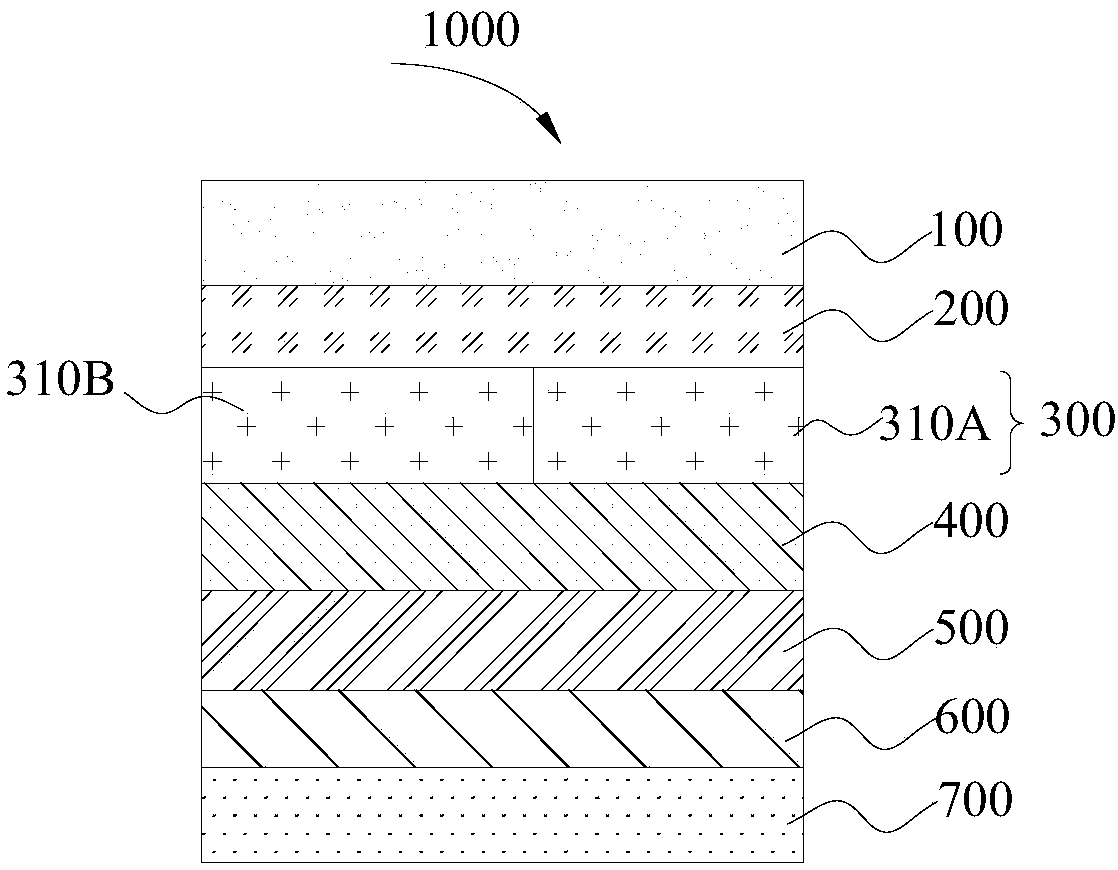
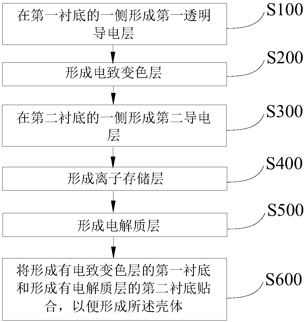
[0020] In one aspect of the invention, the invention proposes a casing. According to an embodiment of the present invention, refer to figure 1 , the housing 1000 includes: a first substrate 100 , a first transparent conductive layer 200 , an electrochromic layer 300 , an electrolyte layer 400 , an ion storage layer 500 , a second conductive layer 600 and a second substrate 700 . Wherein, the first transparent conductive layer 200 is arranged on one side of the first substrate 100, the electrochromic layer 300 is arranged on the side of the first transparent conductive layer 200 away from the first substrate 100, and the electroly...
PUM
| Property | Measurement | Unit |
|---|---|---|
| Thickness | aaaaa | aaaaa |
| Thickness | aaaaa | aaaaa |
Abstract
Description
Claims
Application Information
 - Generate Ideas
- Intellectual Property
- Life Sciences
- Materials
- Tech Scout
- Unparalleled Data Quality
- Higher Quality Content
- 60% Fewer Hallucinations
Browse by: Latest US Patents, China's latest patents, Technical Efficacy Thesaurus, Application Domain, Technology Topic, Popular Technical Reports.
© 2025 PatSnap. All rights reserved.Legal|Privacy policy|Modern Slavery Act Transparency Statement|Sitemap|About US| Contact US: help@patsnap.com